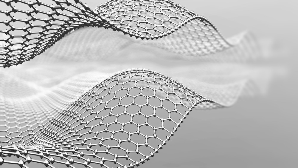
Support grids are a key part of electron microscopy measurements; the choice of the grid can directly influence the quality and accuracy of the final image. This is particularly true for transmission electron microscopy (TEM), where samples must be sufficiently thin to allow for electron beam transmission and reduce unwanted scatter.1 Electron microscopy samples are often too thin to be used without support grids, making these grids an essential part of the experiment design.
Image Credit: Neon_dust/Shutterstock.com
Electron microscopy grids are available in a variety of materials and designs, from regular grid structures to more irregular ‘holey’ or ‘lacey’ structures. Grids are often made from materials such as gold, copper, and silicon, but carbon-based grids also have particular advantages for electron microscopy imaging.2-4
There has been extensive research into developing not just carbon-coated grids but, more specifically, graphene-based grids, particularly for cryogenic electron microscopy (cryo-EM) and imaging of biological samples.5
Graphene Grid Properties
What makes graphene so appealing for use as an electron microscopy grid? As a monoatomically thin layer, graphene substrates are highly uniform.
It is very challenging to avoid any contribution of the grid to the final electron microscopy image, especially as grids can contribute to electron scattering, which can ultimately diminish the effective resolution of the electron microscope. Additionally, depending on the elements involved, certain irregular grid materials can cause poor contrast between the substrate and grid.
Graphene grids facilitate imaging at the atomic layer of surface or interface regions, which is particularly useful when working with functionalized nanoparticles.6
When attempting to image gold nanoparticles with atomic-scale resolution, one research team found that the highly regular, periodic structure of graphene grids allowed them to subtract the grid’s contribution from the final image easily. After image processing, only signals from the substrates of interest remained.
Some graphene grids can even be used to protect samples.7 With the right functionalization, graphene grids can help improve particle distribution across the grid and, when combined with spacers, protect particles from surfaces and environments that may cause oxidation or damage.
Other highly desirable properties of graphene include its inertness. As it is chemically inert, graphene typically does not cause unwanted reactions with the substrate. It can also be specifically functionalized in certain areas to increase its reactivity and intentionally bind particles, which can help improve the particle distribution for imaging.
The very high mechanical strength of graphene is also appealing, as the grids can support any kind of substrate without being negatively affected by the high vacuum conditions inside the electron microscope. This is ideal when combined with graphene’s high thermal stability, which means that it is not easily affected by the intense electron beam conditions of the imaging experiments.
Manufacturing Process of Graphene Grids
There are several different approaches to making graphene or graphene-derivative electron microscopy grids.8 One of the most common ways of producing graphene is through the cleavage or exfoliation of graphite samples, but substrate-free gas-phase approaches can also be used, as well as chemical vapor deposition.8
For some applications, it is sufficient to coat an electron microscopy grid made from another material, such as gold, with a graphene layer.9 It can be challenging to assess the quality of graphene grids, and for research groups that do not have specialists in graphene synthesis, it can also be challenging to make grids efficiently. These are some reasons behind the great demand for simplified synthesis methods.9
Advantages of Graphene-Based Grids
Many of the advantages of using graphene-based grids come from the relatively unique material properties of graphene. It is sometimes described as a ‘near-ideal’ substrate for many cryo-EM applications.9
The high electrical conductivity of graphene helps reduce electron beam charging effects, which can result in image aberrations. High sample charging can deflect the incident electrons and result in worse spatial resolutions. While not immune to electron beam damage or beam-induced reactivity, graphene is reasonably stable.
Future Trends and Potential Applications
Graphene is a popular electron microscopy grid material choice and is becoming increasingly accessible in numerous fields.
A growing number of commercial suppliers now offer a range of graphene grids. These trends are accompanied by improved availability of cryo-EM instrumentation and techniques through consulting services and the development of open-access cryo-EM facilities.
Future areas of development likely include improved targeted functionalization and the ability to create multilayer graphene grids. Targeted functionalization has been shown to improve particle distribution and image quality, as well as provide a means of exploring new chemistry on surfaces.
More from AZoNano: Nanotechnology in Biodiversity Conservation
References and Further Reading
- Franken, LE., Grünewald, K., Boekema, EJ., Stuart, MCA. (2020). A Technical Introduction to Transmission Electron Microscopy for Soft-Matter: Imaging, Possibilities, Choices, and Technical Developments. Small. doi.org/10.1002/smll.201906198
- Sharma, V., Sundaramurthy, A. (2022). Surface modification of bare copper grids with charged polymers: A simple alternative for carbon coated copper grids in transmission electron microscopy. Materials Letters. doi.org/10.1016/j.matlet.2021.131204
- Park, J., Park, J., Lee, S., Roh, SH. (2020). Grid selection strategy for high-resolution cryo-EM. Korean Society for Structural Biology. doi.org/10.34184/kssb.2020.8.2.41
- Last, MGF., Tuijtel, MW., Voortman, LM., Sharp, TH. (2023). Selecting optimal support grids for super-resolution cryogenic correlated light and electron microscopy. Scientific Reports. doi.org/10.1038/s41598-023-35590-x
- Fan, H., Sun, F. (2022). Developing Graphene Grids for Cryoelectron Microscopy. Frontiers in Molecular Biosciences. doi.org/10.3389/fmolb.2022.937253
- Lee, Z., Jeon, KJ., Dato, A., Erni, R., Richardson, TJ., Frenklach, M., Radmilovic, V. (2009). Direct imaging of soft-hard interfaces enabled by graphene. Nano Letters. doi.org/10.1021/nl901664k
- Wang, F., et al. (2020). Amino and PEG-amino graphene oxide grids enrich and protect samples for high-resolution single-particle cryo-electron microscopy. Journal of Structural Biology.. doi.org/https://doi.org/10.1016/j.jsb.2019.107437
- Dato, A., Radmilovic, V., Lee, Z., Phillips, J., Frenklach, M. (2008). Substrate-Free Gas-Phase Synthesis of Graphene Sheets. Nano Letters. doi.org/10.1021/nl8011566
- Ahn, E., et al. (2023). Batch Production of High-Quality Graphene Grids for Cryo-EM : Cryo-EM Structure of Methylococcus capsulatus Soluble Methane. ACS Nano. doi.org/10.1021/acsnano.3c00463


