


If a charged particle beam interacts with structures of different electric conductivity in a microelectronic circuit, this leads to local changes in the electric potential at its surface.
In a scanning electron microscope (SEM), this phenomenon causes a distinct voltage contrast superimposed on the image. This is valuable for failure analysis and device debugging in microelectronic research and development.
When irradiated by the electron beam in the SEM, bulk insulating specimens or insulated layers on a conductive substrate with a thickness exceeding the electron range become charged.
If the combined drain of secondary and backscattered electrons is greater than the supply of primary beam electrons, this causes a positive net charge which creates a positive electric surface potential.
This potential affects the trajectories of primary, secondary, and backscattered electrons, resulting in part of the secondary electrons being unable to reach the detector. This leads to insulated structures being darker in the secondary electron image than grounded structures that do not charge, as displayed in Figure 1.
This occurrence is known as passive voltage contrast. For example, this technique may quickly identify electrical openings in contact chains. Electric surface potentials can also be actively controlled in integrated circuits by applying voltages to selected interconnects.
Following this, the connected structures are visible with different contrast in the secondary electron image. Like passive voltage contrast, positive regions appear dark, while negative regions appear bright, as illustrated in Figure 2.
This active voltage contrast can detect dielectric leakage or metallization shorts. Active elements in the device under test may be dynamically driven, facilitating waveform and timing measurements.
Active voltage contrast on microelectronic devices demands accurate probing with micromanipulators. Interconnects may be contacted with a single microelectrode tip to apply a voltage against the grounded substrate. At the same time, closed electrical circuits may be formed through contact with two or more tips concurrently.
The successful implementation of this method on modern nanoscale interconnects requires tip positioning accuracy in the nanometer range, low backlash, low drift, and insusceptibility to vibrations of the micro-probing setup.
Figure 1. Passive voltage contrast on an integrated circuit. Image Credit: Carl Zeiss Microscopy GmbH
Solution
An SEM with nanometer lateral resolution and high secondary electron detection efficiency is required for voltage contrast on current integrated circuits. Micromanipulators with nanometer accuracy for controlled electrical contacting are also required to adjust surface potentials on circuit structures.
The ultimate lens of the ZEISS GEMINI FE-SEM column is electrostatic and does not enforce a magnetic field on the sample. The trajectories of the emitted electrons are maintained.
The highly efficient in-lens secondary electron detector enables the detection of almost purely secondary electrons based on their trajectories in the column. Both features contribute to a clean and robust voltage contrast on microelectronic structures.
The excellent low-voltage performance of the GEMINI column facilitates the utilization of low acceleration voltages for voltage contrast. This reduces image distortions and contrast artifacts due to excessive local sample charging.
Active and passive voltage contrast may be specifically fine-tuned while preserving the high image resolution.
Micromanipulator devices that meet the requirements for active voltage contrast experiments on state-of-the-art microelectronic structures are available from numerous vendors and easily integrate with ZEISS instruments.
Application Examples
Using an in-lens secondary electron detector, all images presented here were recorded using a memory circuit sample with the GEMINI SEM column at 2 kV acceleration voltage and 5 mm working distance. An example of passive voltage contrast is displayed in Figure 1.
The in-lens secondary electron detector signal generates strong voltage contrast without affecting topography contrast and superposed material contrast from backscattered electrons.
Figure 2 presents a typical active voltage contrast image. Kleindiek Nanotechnik MM3A piezo micromanipulators were employed to generate the examples presented here.
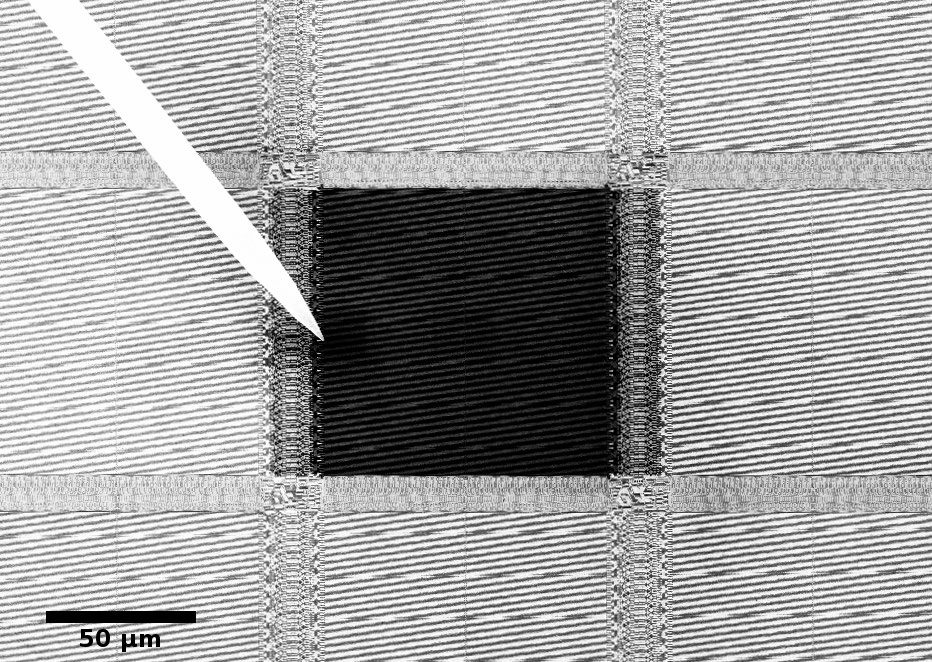
Figure 2. Highlighting an interconnected circuit area by biasing with a microelectrode tip. Image Credit: Carl Zeiss Microscopy GmbH
For the electrical biasing, etched tungsten wire tips were attached to the micromanipulators and connected to a 6 V battery pack.
Figure 3 presents the selective highlighting of an individual 100 nm wide interconnect line, while Figure 4 displays the contacting individual interconnects in a more complex structure.
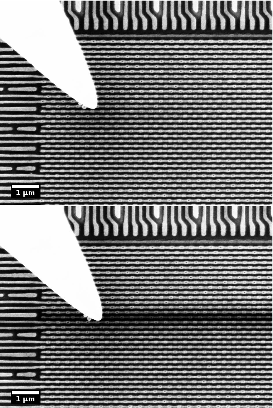
Figure 3. Selective biasing of a single, 100 nm wide interconnect line. Top: Before tip contact. Bottom: Contacting the line. Image Credit: Carl Zeiss Microscopy GmbH
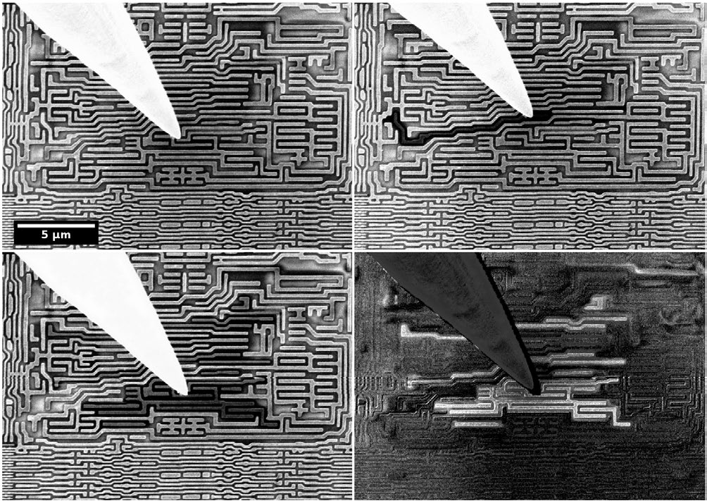
Figure 4. Selective biasing of adjacent interconnects. Top left: Before tip contact. Top right and bottom left: contacting two adjacent lines. Bottom right: Difference image between the two images on the left. Image Credit: Carl Zeiss Microscopy GmbH
Figure 5 shows active voltage contrast with voltage application to the ends of contact chains via two tips. The gradual decrease in voltage along the chains due to its electrical resistance is seen as a gradual decrease of the contrast along the chain structures.
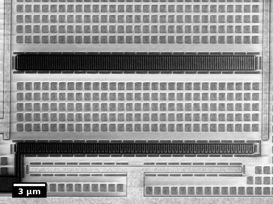
Figure 5. Closed circuit biasing of contact chain structures using two tips (Tips not show in the image). The voltage drop along the chain structures becomes visible as a gradual decrease of voltage contrast. Image Credit: Carl Zeiss Microscopy GmbH
The structural detail of the sample remains fully resolved. Tracing long interconnect lines to locate shorts or opens is significantly assisted by the GEMINI column’s large beam shift option.
The approximate +/-150 µm beam deflection range of the GEMINI enables the movement of the scan field along interconnects at high magnification over a vast distance, as shown in Figure 6.

Figure 6. Montage of seven images recorded by moving the scan along a highlighted interconnect line over more than 90 µm using the large beam shift option of the GEMINI column. Image Credit: Carl Zeiss Microscopy GmbH
Conclusion
As demonstrated by these examples, the ZEISS GEMINI FE-SEM column delivers excellent voltage contrast on microelectronic samples, allowing strong passive voltage contrast to be easily accomplished.
Active voltage contrast experiments that demand the precise contact of interconnect structures may be conducted with a simple and economical micro-probing setup.
An additional advantage of failure localization is the large beam shift option. In many cases, the time-consuming movement of the sample and repeated positioning of the tips can be avoided.
The focused ion beam provides a further means for failure investigation in microelectronic circuits. Structures can float by interrupting their grounding with the ion beam (not shown here). They can be grounded via ion beam cutting and subsequent ion beam-induced metal deposition.
The ZEISS Crossbeam combines SEM and a focused ion beam to enable these operations to be carried out with simultaneous control of the resulting voltage contrast changes using the GEMINI column.
Acknowledgments
Produced from materials originally authored by Dr. Heiko Stegmann at Carl Zeiss Microscopy GmbH.

This information has been sourced, reviewed and adapted from materials provided by Carl Zeiss Microscopy GmbH.
For more information on this source, please visit Carl Zeiss Microscopy GmbH.
