From the inception of the groundbreaking nGauge AFM to the launch of the innovative Redux AFM, David Morris, Director of Operations, shares insights on ICSPI’s mission to enhance accessibility and efficiency in atomic force microscopy, along with their commitment to fostering scientific research and customer support.
Please could you introduce yourself and your role at ICSPI?
My name is David Morris, and I am a Chemical Engineer by training. After completing a Master’s in Nanomaterials from McGill University, I started a research and testing services consultancy called CoLab. I joined ICSPI in 2018 as Director of Operations, where I manage the company’s operations.
Who is ICSPI and what solutions do you offer to the AFM and nanoscale metrology community?
At ICSPI (pronounced “eye see spy”), we design and manufacture powerful and intuitive benchtop AFM systems. Our first instrument, the nGauge AFM, reset the expectations for nanoscale surface imaging. (The nGauge was also featured in one of the most-watched videos about AFM of all time.)
Our mission is to expand access to nanoscale measurement with powerful, automated and intuitive imaging tools. We do this using our unique AFM-on-a-chip technology, which dramatically simplifies and accelerates AFM operation.
Our instruments are used every day in over thirty countries by scientists and engineers to quickly and conveniently collect quantitative nanoscale data, necessary for research, quality control and education.
We are based in Waterloo, Ontario, Canada. All of our systems are assembled in and shipped from Waterloo.
Image Courtesy of ICSPI
ICSPI has recently launched the Redux AFM, an automated benchtop AFM with unprecedented ease of use. Why is this product so exciting for nanoscale surface imaging?
We’re really excited about the possibilities that the Redux opens up for scientists and engineers. One of my favourite articles on this topic is Dalia Yablon’s “After 30 years, AFM can still be frustrating to use”.
For context, she has been using AFMs for over twenty years, and in the article, she describes how even brand-new AFM instruments using the latest technology are still very finicky and can be off-putting for new users.
We agree that legacy AFMs are truly tedious to use. We often hear from researchers that they avoid using AFM and opt for another technique — even if AFM is a better fit for their application and will give them better data.
What is exciting about the Redux is that it makes atomic force microscopy so much more accessible. It’s an AFM that scientists and engineers want to use.
How does the Redux AFM’s versatility make it suitable for sample analyses and applications?
AFM is a versatile technique, but because legacy AFM instruments are so complicated, scientists and engineers often don’t take advantage of AFM’s capabilities and opt for other techniques.
When set-up and scanning are quick, scientists and engineers can use AFM for routine analysis, such as gathering step height, roughness, particle size and distribution, and spatial distribution of components using phase imaging.
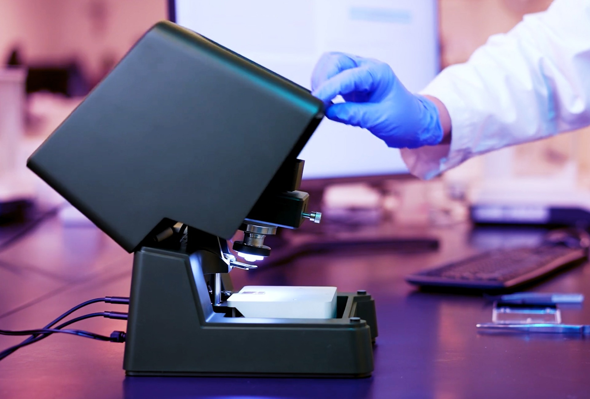
The motorized XYZ stage and integrated optical microscope speed up navigation to a precise region of interest and make it hands-free. The Redux makes routine AFM analysis a possibility for the first time.

Image Courtesy of ICSPI
Why was it important for ICSPI to develop this product for the current AFM market?
Following the success of our breakthrough product, the nGauge AFM, we knew that ease of use and fast time-to-data resonated with scientists, engineers and educators. We wanted to make AFM even easier to use and more automated. We talked to our customers and looked at how we could improve the user experience further; we incorporated this feedback into our roadmap and developed the Redux.
The Redux combines our unique MEMS AFM technology, a precision motorized stage, an integrated optical microscope, and a large sample platform in a benchtop format.

Image Courtesy of ICSPI
Redux AFM also has the fastest time-to-data commercially available. Could you tell us more about how this is achieved?
The time-to-data using the Redux is so short because of our AFM-on-a-chip technology. We discuss how the technology works below, but compared to legacy AFMs, the operation is dramatically sped up and simplified. AFM-on-a-chip technology saves time and effort for users compared to legacy AFMs:
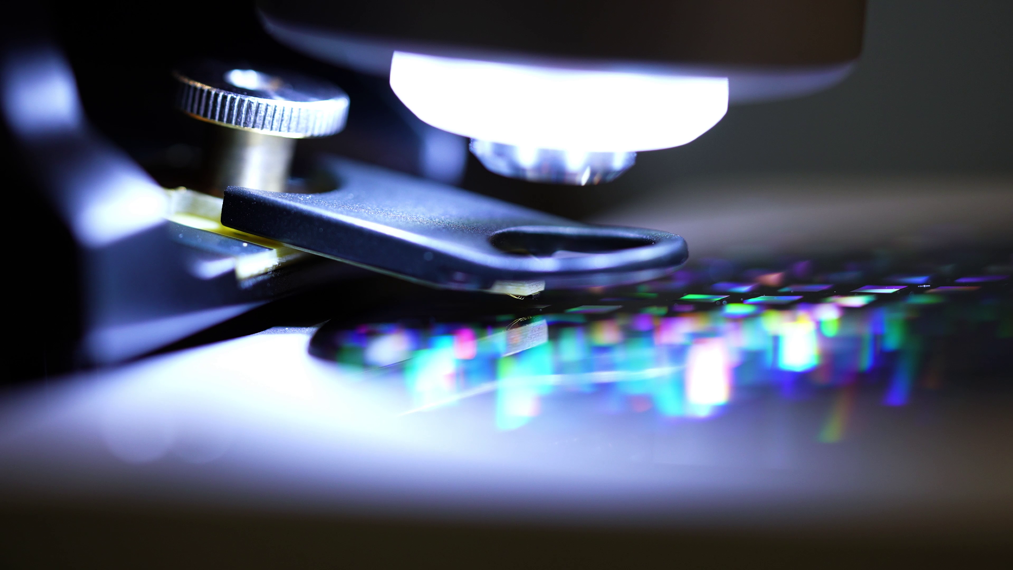
- Easy tip loading: there is no traditional silicon cantilever loading with fine tweezers as our chips are on an easy-to-handle carrier PCB.
- One-click configuration: there is no laser alignment required because there is no laser.
- One-click automatic approach: the approach from the tip to the sample is fully automated.
- Precision sample positioning: the XY sample stage is motorized and an optical microscope is integrated into the system to allow for precise scan area selection.
- Extremely long lifetime probes: our unique chips enable an extremely long lifetime, so it minimizes the number of sample exchanges.
Because the Redux is so easy to use, even users completely new to AFM can collect their first scans in minutes.
Redux AFM is powered by ICSPI’s MEMS-based AFM-on-a-chip technology; how does this work, and why is it different from other devices seem in industry?
Legacy AFMs use miniature silicon probes, complex laser-based detection systems, piezoelectric stages and require multiple manual alignment steps. While advances have been made to AFM instrumentation to achieve higher resolution, faster scan speeds, and more exotic modes, ease of use and time to data have not been priorities.
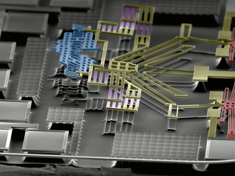
Our AFM-on-a-chip technology simplifies AFM operation in a few ways. AFM-on-a-chip uses micro-electro-mechanical systems (MEMS) technology to incorporate scanning and sensing onto a single chip. Each MEMS chip is capable of extremely precise movement in XYZ for scanning and each chip has built-in sensors for nanoscale measurement and the automatic approach.
In addition to the benefits described above, there are several technical benefits of using MEMS over legacy optical- and piezo-based AFM, such as lower drift, greater vibration immunity, and no hysteresis or creep (a common problem in AFM due to the piezoelectric scanners).
This technology can also be used to boost the throughput of nanoscale measurement in semiconductor manufacturing, as mentioned in this study. Could you tell us more about this research and its findings?
Because each MEMS AFM device is miniaturized to 1 mm2 and manufactured on a wafer, we can manufacture and operate arrays of multiple AFMs simultaneously. In doing so, we can boost the throughput of nanoscale measurement by collecting data in multiple sites from a sample simultaneously.
In this study, we developed the world’s first multi-site AFM array where each device was capable of 3-axis movement and nanoscale measurement. The devices were on a pitch of just over 1 mm, and we demonstrated simultaneous scanning on different structures.
As the features of semiconductor devices get smaller and smaller, higher resolution techniques are needed for semiconductor metrology and inspection. There is usually a trade-off between higher resolution and slower throughput.
We describe the possibility of maintaining high resolution and high throughput for semiconductor metrology by parallelizing AFMs where they operate in arrays. Since each device is so small, tens, hundreds or thousands of AFMs could operate simultaneously, increasing the number of sites scanned across a wafer by 10x, 100x or 1000x.
Collecting more data on each wafer can detect problems and improve yield, saving time, reducing scrap, and enabling faster time-to-market for new products.

Image Courtesy of ICSPI
Why is it important for ICSPI to participate in scientific research, and how does it help the company maintain a close relationship with the academic community?
Many of our users and customers are professors, postdoctoral fellows and graduate students, and we are energized by the passion that they bring to their research.
It’s important to note that many of our users and customers work in corporate research or industrial manufacturing/quality control. By conducting scientific research and participating in technical conferences, we also engage with the industrial scientific community.
Our scientists and engineers push the limits of what’s possible with nanoscale imaging. By contributing to science, we hope to deepen our understanding of the universe and improve quality of life worldwide.
What support does ICSPI offer its customers, such as those using the Redux AFM or other equipment in your product range?
We offer direct support to all of our customers in their research, quality control, and education efforts through our application engineering team. We also work with a network of excellent distribution partners around the world who provide support in their territories.
Where can our readers go to stay up to date with the company’s activities?
Follow us on LinkedIn and sign up for our newsletter on our website.
About David Morris
 David Morris is a Chemical Engineer by training. Following the completion of his Master’s in Nanomaterials from McGill University, he established a research and testing services consultancy known as CoLab. In 2018, he embraced a new role at ICSPI, joining as the Director of Operations, where he oversees the company’s operations.
Disclaimer: The views expressed here are those of the interviewee and do not necessarily represent the views of AZoM.com Limited (T/A) AZoNetwork, the owner and operator of this website. This disclaimer forms part of the Terms and Conditions of use of this website.


