


Refined, high-performance technology often demands electrical components with state-of-the-art material properties [1].
An example of this would be TiO2 thin film, a versatile compound which is extensively used as a high capacity anode for Li-Ion batteries and as a charge selective transport layer in solar cells. This material demonstrates exceptional cycling stability and Coulombic efficiency in contrast to other transition oxides [2] when utilized for battery applications.
Another functional material used in state-of-the-art technology components is SiC, which is applied in power devices to enhance dielectric breakdown field strength, bandgap and thermal conductivity [3].
A creative and accurate nanoscale characterization method for electrical analysis is necessary to enable the battery and semiconductor industries to perform nanoscale electrical measurements throughout the manufacturing process.
Scanning Spreading Resistance Microscopy (SSRM) and Conductive Atomic Force Microscopy (C-AFM) are useful techniques for investigating electrical properties of state-of-the-art materials.
These methods measure electrical properties during topography measurements by monitoring the current flowing between the conductive tip and the sample. Sensitivity in these methods can be greater improved upon by ensuring a controlled measurement environment.
An earlier study demonstrated that utilizing C-AFM in a vacuum environment eradicates the layer of contaminants (water and hydrocarbons) that form on the tip and inhibits oxidation during scanning, enabling an extended lifetime of the tip and enhanced sensitivity [4, 5].
This technical note outlines a study of two separate samples with the Park NX-Hivac atomic force microscope thereby demonstrating the advantage of a high vacuum environment for C-AFM and SSRM measurements.
The results exhibit greater sensitivity and resolution in the measurements under high vacuum conditions in contrast to an ambient air environment.
Experimental
Using a Park NX-Hivac system, two samples are chosen for investigation. The first sample is a Silicon Carbide (SiC) MOSFET and the second sample is a TiO2 thin film deposited onto Au/Ti/SiO2 substrate, henceforth referred to as Sample 1 and Sample 2, accordingly.
Images for Sample 1 are obtained in SSRM Mode utilizing a 0.5 Hz scan rate and a scan size of 1.5 µm x 1.5 µm. Image acquisition for Sample 2 is performed in C-AFM Mode with a scan rate of 1.0 Hz and a scan size of 1.5 µm x 1.5 µm.
Throughout SSRM imaging, a full diamond tip CAMS FDP (nominal spring constant k = 27 N/m) is utilized, while a CDT-Contr (nominal spring constant k = 0.5 N/m) is utilized in C-AFM. Application of a silver paste on top of the sample, as well as on the metal sample holder underneath the sample, ensures electrical connection from the bias line.
To determine the environmental impact on C-AFM and SSRM measurements, the samples are measured in both ambient air and vacuum (in the low 10-5 Torr range) conditions. C-AFM and SSRM function in the Contact mode regime and their imaging standards are reasonably comparable.
When applying DC bias, the flow of the current between the conductive tip and sample is observed, and the electrical properties are measured. The conductive tip serves as an electrode.
It is necessary to include a current amplifier to boost the current signal as the current typically has an extremely low magnitude. For subsequent image processing, the current amplifier both enhances and monitors the current.
Throughout experiment, the DC bias is +2.5 V for Sample 1 and +4 V for Sample 2. The major differences between the two methods are their applications and the type of current amplifiers necessary. SSRM measures a surface’s conductance and local resistance, whereas C-AFM is frequently utilized for current variations mapping.
The SSRM mode of Park Systems utilizes a logarithmic current amplifier to measure an extensive range of resistance distribution in a small area. Comparatively, C-AFM mode utilizes a linear current amplifier.
Figure 1. Schematic Illustration of C-AFM and SSRM AFM. Image Credit: Park Systems
Figure 1 displays a schematic view of a C-AFM and SSRM set-up on the Park NX-Hivac system. The AFM cantilever tip, coated with a conductive material, connects to a current amplifier and as a result has the ability to measure an extensive range of current signal.
The electric current flow is measured at the tip-sample contact point by the current amplifier. Similar to other AFM modes, the super luminescent diode (SLD) light beam and position sensitive photodiode (PSPD) act as feedback (Feedback Control) to determine topographic features.
To acquire the topography and electrical current C-AFM or SSRM image, the AFM controller then measures and processes any changes.
Results and Discussion
Figure 2 shows topography and resistance images of Sample 1 acquired in ambient air and high vacuum while utilizing SSRM mode. In Figures 2a and 2b the topography images display a polished surface with a height difference of 109 nm on the cross-section.
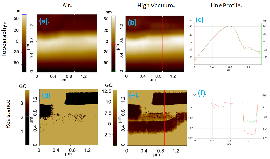
Figure 2. Topography and resistance images measured on a SiC MOSFET sample in ambient air and high vacuum using SSRM mode. (a) Topography in air (b) and vacuum (c) and the corresponding line profiles. (d) Resistance image in air (e) and vacuum (f) and the corresponding line profiles. Image Credit: Park Systems
Yet, they do not hold important information relative to the device pattern.
As shown Figure 2c, the matching topography line profiles exhibits how the measurement positions in both images are equal in ambient air and in high vacuum conditions. This means it is possible to conduct environmental comparison.
Figures 2d and 2e are the resistance images taken at the same time as the topography images in Figures 2a and 2b, respectively.
By Figures 2d and 2e, the resistance image captured in high vacuum exhibits better features and details than the one taken in air. In fact, line profiles of the resistance images, as displayed in Figure 2f, show a considerable shift in the resistance distribution in air and vacuum.
Since no oxidation or water layer is present in the vacuum, the SSRM exhibits a greater sensitivity in a vacuum than in air due to the enhanced electrical contact between the tip and sample. Characterizing electrical properties with this level of detail is crucial for determining the functionality of a MOSFET device.
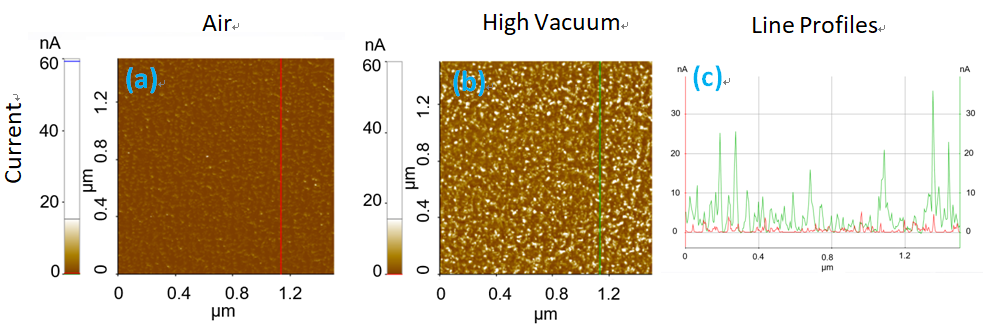
Figure 3. Current images measured in TiO2/Au/Ti/SiO2 sample in ambient air and high vacuum using C-AFM mode. (a) Current image in air (b) and vacuum (c) and the corresponding line profiles. Image Credit: Park Systems
Figure 3 provides the current images of Sample 2 as acquired in ambient air and high vacuum while utilizing C-AFM mode. Small grain-structures with different contrasts are apparent in the current image acquired in high vacuum, while the current image in air exhibits less detail.
The maximum current observed in high vacuum is 827 nA, while in air it is 59 nA.
The line profiles of the current images, as exhibited in Figure 3c, corroborates the theory that a consistently greater current is measured in high vacuum than in air. This enhanced electrical sensitivity in high vacuum is possibly due to the elimination of water and contaminants that are usually present on the sample surface in air.
Conclusion
This application note analyses the existing image quality of the SSRM and C-AFM modes of the Park NX-Hivac atomic force microscopy system.
To investigate the sensitivity of electrical measurements using both modes, two samples, a SiC MOSFET and a TiO2/Au/Ti/SiO2, are tested under ambient air and high vacuum conditions.
In high-vacuum environments the sensitivity of the electrical characterization increases, as demonstrated in the results. The residues tend to be insignificant in a high vacuum, which enhances the electrical contact at the tip-sample surface.
Thus, the current can circulate more freely and reveal the current contrast of smaller features with a greater definition. In conclusion, operating the Park NX-Hivac system in high vacuum provides comprehensive insights for different nanotechnology applications and enables an enhanced understanding and control of the electrical behavior of state-of-the-art materials and devices at the nanoscale.
References
- Puetz, et al., Characterization of Electrical Properties. DOI: 10.1007/978-3-319-19454-7_52-1
- M. Madian, et al., Current Advances in TiO2-Based Nanostructure Electrodes for High Performance Lithium Ion Batteries.
- ROHM Semiconductor, SiC Power Devices and Modules Application Note. Issue of August 2014 14103EBY01
- L. Aguilera, et al., Influence of vacuum environment on conductive atomic force microscopy measurements of advanced metal-oxide-semiconductor gate dielectrics. DOI: 10.1116/1.2958246.
- J. Ludwig, et al., Advantages of High Vacuum for Electrical Scanning Microscopy. https://parksystems.com/images/media/appnote/App_Note_36_Advantages-of-High-Vacuum-for-Electrical-Scanning-Probe-Microscopy_correctionsIH_JS_1.pdf

This information has been sourced, reviewed and adapted from materials provided by Park Systems.
For more information on this source, please visit Park Systems.
