


The interaction volume of a characteristic X-Ray emission can be seen in Figure 1. Typical EDS analysis in an SEM is carried out at relatively high energy (greater than 10 kV), which results in a vast interaction volume in the order of micrometers.
Figure 1. Schematics comparing the interaction volume of X-ray emission in an SEM between high energy bulk, low energy bulk and high energy transmission. Image Credit: Carl Zeiss Microscopy GmbH
Decreasing the energy of the primary electron beam allows the interaction volume to be significantly reduced. Aided by a specifically designed detector, EDS analysis with a beam energy down to 1 kV is viable, exhibiting nanometer-scale resolution.1
However, low-energy EDS presents numerous practical challenges. One example is X-Ray emission with low electron beam energy having a considerably low yield. This results in low count rates during analysis.
Low-energy X-Ray lines, including M and N lines, must be used for higher atomic numbers.
Typically, these low-energy X-Ray emission lines have complex shapes and are extremely challenging to quantify. An extremely clean specimen is required due to the high surface sensitivity of low-energy EDS.
An alternative technique to decrease the interaction volume is using a thin sample. For example, in a transmission scanning electron microscope, the sample thickness is decreased to tens of nanometers to make it effectively transparent to the electron beam during imaging.
However, STEM-EDS advantages from the high energy of the primary electron beam to excite K or L lines, which are easy to quantify. A practical challenge for STEM-EDS is the stray X-Ray signal.
In a STEM configuration, most electrons penetrate the specimen and reach different parts of the SEM system. This results in pronounced stray X-Ray signals, particularly from Al and Si K lines, created from the SEM stage and the STEM detectors.
To reduce this stray X-Ray signal, a collimator can be utilized to restrict the incoming X-Rays’ acceptance angle to be restricted by the EDS detector.
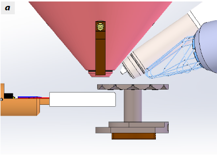
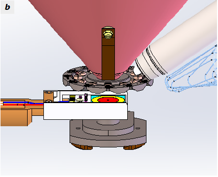
Figure 2. Comparing a favorable (a) and unfavorable (b) configuration for an EDS analysis with STEM. Under the favorable configuration, the STEM sample holder blocks the stray X-Ray signal from the detector and sample chamber. Image Credit: Carl Zeiss Microscopy GmbH
The specimen holder for the STEM samples can also be used for blocking the stray X-Ray signal, as presented in Figure 2. There are several potential configurations to position the STEM specimen against the STEM detector, but only one optimum configuration for blocking the stray X-Ray signal.
In this optimal configuration, the STEM specimen holder is positioned immediately beneath the EDS detector and above the STEM detector. This blocks the direct line of sight between the EDS detector and the rest of the SEM chamber, preventing the stray X-Rays from entering the EDS detector.
The efficacy of this optimal configuration is illustrated in Figure 3.
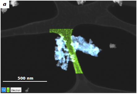
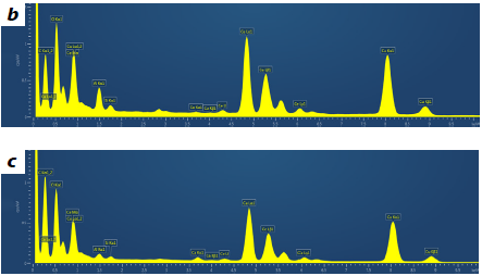
Figure 3. High-resolution EDS mapping of CeO2 nanoparticles deposited on a carbon grid measured at 30 kV. The corresponding EDS spectrum was obtained in two different configurations. In the favorable configuration (c) the stray signal from the STEM detector/sample chamber is reduced. Image Credit: Carl Zeiss Microscopy GmbH
The test specimen is comprised of CeO2 nanoparticles that are deposited on the lacey carbon on a copper grid. The elemental mapping shows the high spatial resolution of STEM-EDS analysis.
The same analysis is carried out with favorable and unfavorable configurations. In comparing the two EDS spectra, it can be seen that the stray signals from Al and Si are significantly suppressed in the favorable configuration.
The STEM-EDS method is especially suitable for nanomaterials. Nanomaterials are transparent to a high-energy electron beam due to their nanometer-scaled size in at least one of their dimensions. This means they can be prepared by simply dispersing them on a typical copper grid with a carbon film.
Figure 4 presents an example where the Co nanoparticles are dispersed in mesoporous silica and are imaged at 30 kV in high angular dark field mode. The Co nanoparticles have an average size of approximately 10 nm and are deposited inside the nanometer-sized channels of mesoporous silica.
The elemental mapping displayed in Figure 4 shows the capability of STEM-EDS to resolve nanometer-scale objects even smaller than 10 nm.
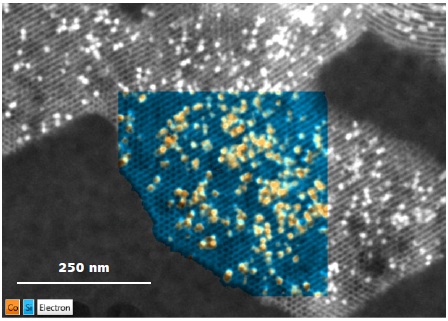
Figure 4. High-resolution EDS mapping of Co nanoparticles embedded in mesoporous silica measured at 30 kV. Individual Co nanoparticles with approx. 10 nm sizes are resolved. Image Credit: Carl Zeiss Microscopy GmbH
Acknowledgments
Produced from materials originally authored by Luyang Han at Carl Zeiss Microscopy GmbH, Germany.
References and Further Reading
- Nanometer scale EDS Analysis using Low-kV FE-SEM and Windowless EDS Detector, Technology Note ZEISS.

This information has been sourced, reviewed and adapted from materials provided by Carl Zeiss Microscopy GmbH.
For more information on this source, please visit Carl Zeiss Microscopy GmbH.
