


Piezoelectrical materials are utilized in various applications, from biomedical (cardiac, auditory, ultrasound, and numerous biosensors) to advanced electronics—including energy production and storage, information storage, sonar equipment, micro-electromechanical systems (MEMS).
Piezoelectricity refers to the capability of specific solid materials to create an internal electric field when subjected to mechanical stress or strain. These materials can exhibit the reverse piezoelectric effect, producing mechanical strain when introducing an electric field.
The electrical field produced when a piezoelectric material is exposed to pressure can be utilized to create an electric current in energy harvesting devices or to transform an acoustic signal into an electric signal, as seen in microphones.
In the reverse piezoelectric effect, applying a voltage to the piezo material creates the electrical field, which modifies the volume and dimensions of the material, such as the length. This property is utilized in various applications, including actuators like atomic force microscopy (AFM) scanners.
Numerous piezoelectrical materials are also ferroelectrics. In other words, they can be electrically polarized.
Piezoresponse force microscopy (PFM) is a tool for fundamental research studies and the practical application of a wide range of ferroelectric materials and multiferroics, along with several devices leveraging piezoelectric effects.
PFM enables the imaging of electric polarization domains and facilitates the characterization and imaging of domain switching (reversal)—that is, the determination of parameters like reversal nucleation, remanent polarization, and coercive field (voltage).
Nanosurf’s software incorporates comprehensive PFM functionality, enabling the analysis of both out-of-plain and in-plain PFM responses of a sample. This functionality can be expanded with an advanced external lock-in amplifier, further augmenting PFM analysis. This article explains dual-frequency-resonance-tracking (DFRT) PFM utilizing a Zurich Instruments lock-in amplifier.
Standard PFM Techniques
Various PFM implementations exist. They all apply an AC (alternating current) voltage between the sample and the conductive tip in contact with the sample’s surface. The amplitude and phase of the cantilever deflection at the same frequency are identified with a lock-in amplifier.
In the simplest case (“off-resonance PFM”), the measurement is conducted at a frequency substantially lower than the cantilever contact resonance. This approach enables the measurement of polarization perpendicular to the electrical field (in-plane) and along it (out-of-plane).
However, this technique typically produces a moderately weak signal (~ pm/VAC), frequently necessitating the application of a high AC excitation voltage to achieve reasonable measurements. The heightened voltage can influence the local polarization and may even induce a change in direction in thin films or materials with low coercive fields.
The AC excitation can be applied at the contact resonance (CR) frequency, which intensifies the piezoelectric response to enhance signal strength. As a result, a substantially lower AC excitation voltage can be employed for the measurements.
However, as the contact resonance frequency is sensitive to the local mechanical tip-sample interaction, surface features may be observed in the measured signal. Numerous factors can influence the CR frequency, such as adhesion, sample elasticity, scanning speed, changes in force set point, humidity, and temperature.1
When PFM measurements are conducted at a fixed resonance or near-resonance excitation frequency, fluctuations in the contact resonance frequency impact the phase and amplitude of the piezo response.
DFRT
The DFRT method was developed to leverage the signal amplification of CR PFM while mitigating concerns about CR frequency variations across the sample or as a function of time.2,3
With the DFRT method, the cantilever undergoes excitation at three frequencies. Alongside the AC excitation at the CR frequency, AC excitation is applied at two “sideband” frequencies on both sides of the CR frequency, equally spaced from that at a fixed distance, approximately full-width-half-maximum of the CR peak.
The amplitudes of the cantilever deflection signal at these sideband frequencies are tracked. The disparity between them is utilized as feedback to control the three excitation frequencies simultaneously. Maintaining equal amplitudes of the sidebands ensures that the excitation frequency (fCR) is tuned to the contact resonance.
Figure 1. Schematic of DFRT principle. (a) Initial contact resonance and the three excitation frequencies (f CR, fCR – fm, and fCR + fm); V(fCR – fm) = V(fCR + fm). (b) As the resonance shifts (dashed light blue line) the amplitudes of the sidebands are no longer the same, V(fCR – fm) < V(fCR + fm). (c) Using the difference V(fCR – fm) – V(fCR + fm) as feedback, the PID controller in the lock-in amplifier shifts all three excitation frequencies (f CR, fCR – fm, and fCR + fm) so that the sideband amplitudes are the same again, V(fCR – fm) = V(fCR + fm). Image Credit: Nanosurf AG
DFRT Setup
A standard DFRT configuration involves identifying the contact resonance frequency (fCR) and configuring the lock-in amplifier to produce excitations at two sideband frequencies (f – =fCR – fm and f +=fCR + fm), where fm is selected to be approximately half the width of the CR peak at half maximum (HWHM).
The sideband excitations are positioned on the shoulders of the contact resonance peak. Thus, their amplitudes are sensitive to the shift of the resonance in frequency, which facilitates effective tracking of the resonant frequency.
The difference of the sideband amplitudes—V(fCR + fm) – V(fCR – fm)—is utilized as feedback to alter the primary excitation frequency and sideband frequencies, effectively tracking the resonance frequency (as shown in Figure 1).
Figure 2 shows a schematic of the DFRT PFM measurements setup.
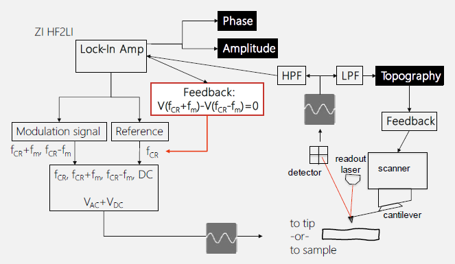
Figure 2. Schematic of DFRT PFM measurements. HPF and LPF are high- and low-pass filters, respectively. Image Credit: Nanosurf AG
Examples of DFRT-PFM Measurements and Lithography
The following presents measurements conducted on a thin film of BaTiO3, utilizing the Nanosurf DriveAFM system in conjunction with a Zurich Instruments HF2LI lock-in amplifier.
BaTi03 was the first polycrystalline ceramic material found to exhibit ferroelectricity. More recently, there has been heightened interest in lead-free piezoelectric BaTi03 and its derivatives.4
Thin films of these materials provide various qualities, including low-voltage switching of ferroelectric domains.5 This, coupled with the lower piezoresponse of thin films compared to the bulk materials, establishes DFRT-PFM as a suitable choice for characterizing ferroelectric switching in such samples.
Figure 3 shows the sample topography measured during the DFRT-PFM imaging. The sample is smooth, exhibiting terraces with an approximate height of 1 nm.
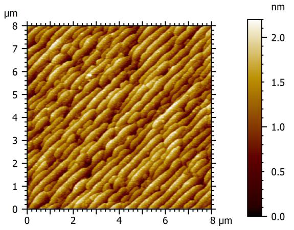
Figure 3. Topography of the BaTiO3 sample. Image Credit: Nanosurf AG
a) Box-in-box PFM Lithography
To illustrate ferroelectric switching, a box-in-box pattern was employed, featuring nested squares of the opposite electric polarizations. The pattern shown here was generated by sequentially scanning the squares with decreasing dimensions while swapping the DC (direct current) voltages added between the tip and the sample for the squares: -5 V for the 5-µm square, +5 V for the 4-µm square, and -5 V again for the 3-µm square.
The final 8 µm × 8 µm image was acquired utilizing a 1 V AC excitation voltage.
The PFM phase is shown in Figure 4 (a), revealing a distinct 180⁰ difference between the phases of the two electrical polarization domains. This is also highlighted by the profile acquired through the sample’s center, averaged over the width of 20 pixels (shown in Figure 4 (b)).
The amplitude and corresponding profile through the center of the image are depicted in Figure 4 (c) and (d), respectively. 6,7 A slight amplitude difference in the opposing polarization domains is credited to the electrostatic charging of the sample surface, as established by the subsequent KPFM measurement. For a potential approach to address the effect of charging, see reference eight.8
No apparent crosstalk from the sample’s topography is evident in the phase or amplitude images.
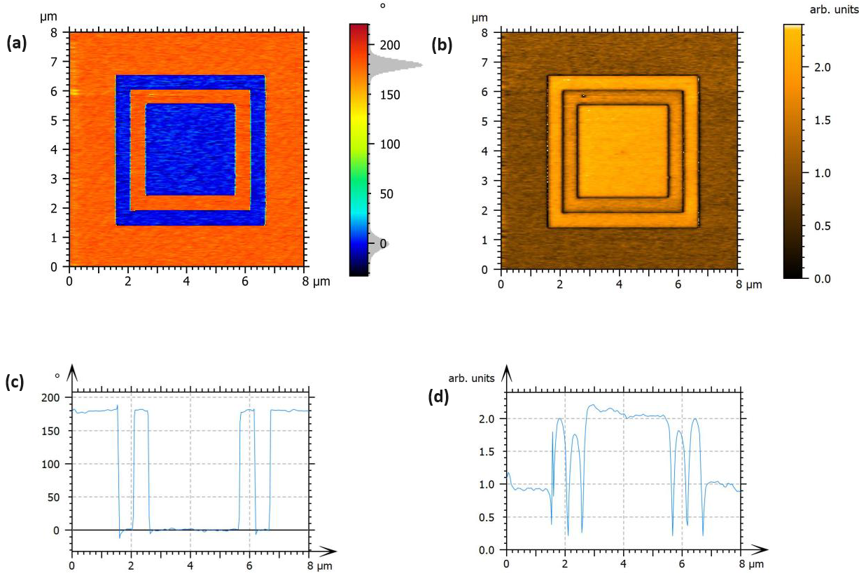
Figure 4. (a) PFM phase of the BaTiO3 thin film after writing a “box-in-box” pattern by sequentially applying DC bias of -5 V, +5 V, and -5 V for 5-, 4-, and 3-μm squares, respectively. (b) PFM amplitude. (c) and (d) Profiles of the PFM phase and amplitude along the horizontal line through the image center in (a) and (c) respectively, averaged over 20-pixels width. Image Credit: Nanosurf AG
b) Arbitrary-Pattern PFM Lithography
As a result of the small size of the ferroelectric domains in BaTiO3, arbitrary images can be written with high resolution utilizing the same method used for the box-in-box pattern.
The PFM phase of the box-in-box pattern with the Nanosurf logo in the middle is shown in Figure 5. To write it, following the box-in-box pattern, a + 5 V DC bias was utilized to generate another domain with opposite polarization (represented by the orange pattern in the center).
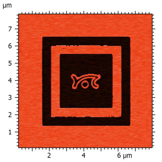
Figure 5. PFM phase image of Nanosurf logo. Image Credit: Nanosurf AG
Additional Considerations for Applying the Voltage
In all PFM techniques, voltage can be applied in two ways: either to the probe or to the sample. Each technique provides specific benefits from instrumental factors and the material’s underlying physics.
The phase of the PFM signal may alter because of any further impedance introduced in the circuit. When complex impedances are added as vectors, it can produce a non-trivial modification of the phase, leading to a non-180° phase difference between domains of opposite polarization.6,7
When the excitation signal is added to the tip, contributions from the scan head, additional impedance, or crosstalk from other signals could influence the phase.
Another factor is the difference in propagation and nucleation of the polarization reversal domains. As domain wall propagation and polarization switching are often stochastic processes, the trajectory of the polarization reversal domain’s propagation may vary when the DC voltage or excitation is applied to the sample or the tip.9,10 This may influence the switching parameters, like the coercive field (voltage).
In numerous PFM characterizations, such as DFRT-PFM, conducting PFM with the voltage applied both ways and comparing the results to recognize and discern potential artifacts may be beneficial.
Summary
DFRT PFM can acquire high-fidelity PFM images utilizing contact-resonance-based signal enhancement while reducing crosstalk with the surface topography. It also removes the necessity for manual retuning of the resonant frequency when environmental conditions (such as temperature) or measurement conditions fluctuate.
Researchers aiming to improve the signal-to-noise ratio (SNR), reduce the excitation voltage, or enhance the reproducibility of their PFM measurements, including Switching-Spectroscopy PFM, stand to gain from utilizing DFRT PFM.
References and Further Reading
- C. C. Glover, Investigation of a Contact Resonance Atomic Force Microscopy Scan Speed Phenomenon, M.S. Thesis, University of Nevada, Reno, 2018.
- B. J. Rodriguez, C. Callahan, S. V. Kalinin, and R. Proksch, Nanotechnology 18, 475504 (2007).
- Zurich Instruments Application Note – Dual-Frequency Resonance Tracking (DFRT), https://www.zhinst.com/en/applicat ions/scanning-probemicroscopy/dual-frequencyresonance-tracking-dfrt.
- M. Acosta, N. Novak, V. Rojas, S. Patel, R. Vaish, J. Koruza, G. A. Rossetti Jr., and J. Rödel, Appl. Phys. Rev. 4, 041305 (2017).
- Y. Jiang, E. Parsonnet, A. Qualls, W. Zhao, S. Susarla, D. Pesquera, A. Dasgupta, M. Acharya, H. Zhang, T. Gosavi, C.-C. Lin, D. E. Nikonov, H. Li, I. A. Young, R. Ramesh, and L. W. Martin, Nat. Mater. 21, 779 (2022).
- P. Buragohain, H. Lu, C. Richter, T. Schenk, P. Kariuki, S. Glinsek, H. Funakubo, J. Íñiguez, E. Defay, U. Schroeder, and A. Gruverman, Adv. Mater. 34, 2206237 (2022).
- S. M. Neumayer, S. Saremi, L. W. Martin, L. Collins, A. Tselev, S. Jesse, S. V. Kalinin, and N. Balke, J. Appl. Phys. 128, 171105 (2020).
- H. Tan, J. Lyu, Y. Sheng, P. Machado, T. Song, A. Bhatnagar, M. Coll, F. Sánchez, J. Fontcuberta, and I. Fina, Appl. Surf. Sci. 607, 154991 (2023).
- A. N. Morozovska, S. V. Svechnikov, E. A. Eliseev, S. Jesse, B. J. Rodriguez, and S. V. Kalinin, J. Appl. Phys. 102, 114108 (2007).
- A. N. Morozovska, E. A. Eliseev, and S. V. Kalinin, Appl. Phys. Lett. 89, 192901 (2006).

This information has been sourced, reviewed and adapted from materials provided by Nanosurf AG.
For more information on this source, please visit Nanosurf AG.
