Traditional semiconductors such as Si, GaAs, and HgCdTe seem unable to meet the development trend of electronic devices that feature ultra-small volume, lightweight, and low power consumption. These limitations of traditional semiconductors mainly stem from complex growth conditions and low-temperature working environments.
In recent years, novel 2-dimensional (2D) materials have provided decent opportunities to develop room-temperature, high-speed, ultra-sensitive, and broadband photodetectors because of their unique structures and excellent physical characteristics. However, the atomic thickness of 2D materials has unavoidably brought about the problem of low light absorption.
One promising solution is the combination of plasmonic nanomaterials with 2D materials for enhanced light-matter interaction, which has already become a research focus. The excitation of surface plasmons in noble metals enables locally amplified electromagnetic fields that can improve light absorption in nearby semiconductors by orders of magnitude. Additionally, the decay of surface plasmons effectively generates hot carriers with high energy.
The hot carriers injected into 2D materials not only increase the photocurrent collected by electrodes but also expand the detectable wavelengths beyond the semiconductor bandgap.
In order to comprehend these hybrid structures and mechanisms, a systematic overview is necessary to extract and summarize the design strategies of plasmon-enhanced 2D material photodetectors, which may provide comprehensive guidance for clarifying the advantages and drawbacks of each strategy and thereby optimizing plasmon-assisted photodetection in future work.
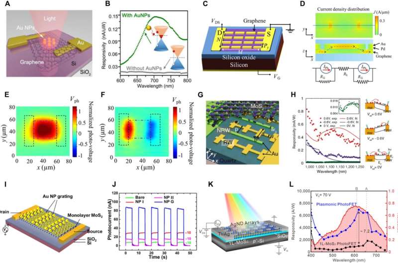
A research group from Southeast University provided a detailed overview of plasmon-enhanced 2D material photodetectors, mainly focusing on the clarification of different hybridization modes between plasmonic nanostructures and 2D materials. The mechanisms of plasmon-enhanced photodetection were introduced in the first section.
Then, they discussed different structure-related coupling modes of the hybrid systems, which are roughly classified into LSPR-guided mode, SPP-guided mode, and other hybrid photonic modes, respectively. Finally, they briefly outlined the problems remaining to be addressed and potential directions in future research work.
In this review, the current design strategies that are adopted for the actualization of plasmonic enhancement in 2D material photodetectors are summarized. Plasmonic nanostructures are widely employed based on LSPR-induced plasmonic effects, either in the form of single-layer plasmonic nanostructures working in different modes (such as direct contact, separated, or embedded mode) or cavity-coupled plasmonic resonators supporting gap-mode plasmonic resonance.
Key factors that can influence light-matter interaction and carrier transport characteristics in the hybrid photodetectors are discussed, including materials, shapes, arrangements, and placements of plasmonic nanostructures.
In addition, patterned plasmonic structures such as stripes, nanogaps, and gratings support the propagating SPP waves that are confined at the near field of the metal surface, facilitating the enhanced energy coupling between metal and 2D materials within a long propagation distance.
When SPP-based metal electrodes are employed, light energy far from the 2D material channel can be effectively collected and absorbed. Moreover, the synergism of other functional photonic structures/materials and plasmon-enhanced 2D material photodetectors is also introduced, resulting in improved performance and novel functionalities.
Plasmon-assisted 2D material photodetectors improved by the above strategies hold great potential for boosting remarkable advancements in wide application fields.
Several potential research directions that may be beneficial for the future development of plasmon-enhanced 2D material photodetectors are proposed.
First, there are still many aspects worth exploring about the plasmonic structures. Despite the fact that researchers have already studied the influence of structural parameters (morphology, density distribution, etc.) on the performance of 2D material photodetectors, internal factors such as crystal quality have not been fully explored yet.
Second, the above strategies have reported various different working mechanisms dominated by the integrated plasmonic materials, while matched physical models and applicable conditions for these plasmonic effects have not been fully clarified, which is necessary to expand these fascinating concepts from laboratory research to commercial devices.
Third, the interface engineering between metal and 2D material has not been fully explored in plasmonic/2D material hybrid structures.
The work is published in the journal Advanced Devices & Instrumentation.
Provided by
Advanced Devices & Instrumentation

