For decades, traditional lithography techniques—such as electron beam lithography and nanoimprinting—have struggled to meet the demand for ultra-fine, high-aspect-ratio structures in general. Similar difficulty also applies to metal-based radio-frequency (RF) components. Issues like poor thickness control, uneven sidewalls, and material limitations have constrained performance and scalability.
Two-photon polymerization (2PP), known for its nanometer-scale precision and 3D design capabilities, has emerged as a promising alternative. However, integrating 2PP with robust metallization for functional RF components remains elusive due to process incompatibilities. Bridging this gap has become critical for enabling compact, high-frequency devices that can meet the evolving needs of wireless communication, material sensing, and chip-level integration.
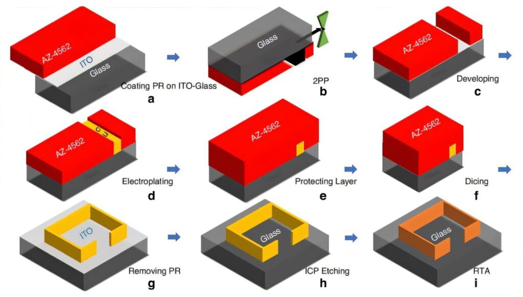
In an article published in Microsystems & Nanoengineering, researchers from Bilkent University and Nanyang Technological University introduced a novel fabrication process that marries nanoscale 3D printing with advanced metal processing. Their approach uses 2PP to create intricate deep trenches, which are then filled with copper via electroplating and refined through dry etching.
The result is ultra-compact RF resonators with tunable frequencies between 4 and 6 GHz, a 1:4 aspect ratio, and exceptional quality factors (Q-factors)—all within a sub-10 µm resolution framework. This milestone represents a major advance in the fabrication of next-generation RF and metamaterial components.
At the core of this study is a precision-engineered workflow combining additive and subtractive techniques. The process begins with 2PP to define high-aspect-ratio trenches in a photoresist layer. These voids are then filled with thick copper—up to 8 µm—through electroplating.
Subsequent dry etching removes seed layers, yielding freestanding metal structures with flat, vertical sidewalls and remarkable dimensional accuracy. The team demonstrated microstructures as narrow as 2–3 µm in width and over 10 µm in height.
Performance-wise, the results are striking. By tuning the geometry—especially increasing metal thickness—the Q-factor improved six to sevenfold, and resonance frequencies shifted by up to 200 MHz, allowing precise tailoring for specific RF applications. Compared with conventional PCB-fabricated resonators, the 3D-printed versions maintained performance while shrinking their footprint by 45%.
To ensure structural stability, rapid annealing was used to strengthen copper bonds, addressing thermal and mechanical challenges. Scanning electron microscopy (SEM) verified the high fidelity of the structures, confirming their robustness and manufacturability. With this technique, the limitations of planar lithography are overcome, opening a new frontier for compact, high-performance RF metastructures and miniaturized electronics.
“This work bridges a critical gap between 3D printing and functional RF devices,” said Prof. Hilmi Volkan Demir, senior author of the study. “By achieving sub-10 micron resolution in high-aspect-ratio metal structures, we’ve unlocked new design freedoms for miniaturized, high-performance components. The ability to tune resonance frequencies and Q-factors through geometric control offers exciting opportunities for next-generation sensors and communication systems.”
This fabrication breakthrough is poised to reshape industries that demand ultra-compact, high-precision components. In wireless sensing, it could enable miniature RF sensors with superior sensitivity. In biomedical technology, the technique may lead to implantable or wearable micro-devices for diagnostics and therapy. Integrated with MEMS, it could revolutionize on-chip antennas and signal processors for IoT networks.
Unlike traditional lithography, this method is scalable and cost-effective, promising broader accessibility for industrial deployment. Future directions include integrating other functional materials or building multi-layer structures to expand device capabilities.
As demand surges for smaller, smarter electronics in fields like 5G, aerospace, and smart wearables, this innovation sets a new standard for what’s possible in micro- and nano-scale RF engineering.


