


In a photovoltaic, semiconductor, and hard disk drive manufacturing industries, the ability to identify nanoscale-sized areas of high and low conductivity is crucial. With an ever-growing requirement to further decrease the size of these products, industries constantly develop new processing steps to fulfill these needs.
More and more devices with critical dimensions become the standard on the market as a result of this. Features which are so small that bulk property values can no longer predict their behavior, face a challenge for the optimizations and the failure analysis of the technology1.
In these instances, by measuring the conductivity on a nanometer scale simultaneously to the sample’s topography, conductive atomic force microscopy (C-AFM) can help to assess those properties2.
The nanoscale current distributions can be correlated with specific observed spatial features by applying a bias between a conductive tip and the sample while scanning the surface.
A schematic view of a C-AFM set-up on the Park NX10 (courtesy Park Systems) can be seen in Figure 1. Coated with a conductive material, the AFM tip is connected to a current amplifier to measure a large range of a current signal.
Figure 1. Schematic view of the Conductive AFM set-up. While the topography feedback is run over the z scanner with keeping a constant laser deflection on the PSPD and, therefore, a constant tip-sample force, the tip-sample current is amplified and recorded under a constant sample bias.
The laser and a position-sensitive photodiode (PSPD) serves as feedback to detect topographic features and the current amplifier measures the electric current flow at the tip-sample contact point, as in other AFM modes.
In this article, topography and electric current data gathered, using a Park Systems NX10 AFM to characterize a polymer sheet sample embedded with carbon nanotubes (CNTs), is discussed. CNTs are extremely strong, in addition to being electrically and thermally conductive.
A small number of CNTs added to polymer matrices create composites with novel mechanical and electrical properties and are widely used in academic and industrial research3, 4. By utilizing C-AFM, it is possible to image both topography and current distribution on the surface of a CNT-polymer composite sheet simultaneously.
Materials and Methods
Sample
For the C-AFM measurement, a customized CNTs embedded polymer sheet was prepared with 80 ohm ~ 90 ohm of electrical resistance measured via multimeter.
So that the top surface of the polymer sheet is connected with the sample bias line through the metallic sample holder, the polymer sheet sticks to a metal sample disk by silver paste, as seen in Figure 2.
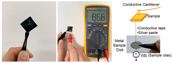
Figure 2. CNTs embedded polymer sample preparation for C-AFM measurement. The macroscopic conductive polymer sheet is stuck on a metal disk with silver paste and thereby provides the electrical connection to the sample bias line.
C-AFM Set-up
With the C-AFM mode, high-resolution topographic data and current signals can be acquired simultaneously by utilizing an AFM tip coated with a conductive material. A platinum-iridium coated tip with 25 kHz of resonance frequency and 0.2 N/m of spring constant (PPP-ContSCPt, Nanosensors) was used in this study5.
All measurement parameters were performed under ambient conditions and were held constant – image size: 1 µmx1 µm and 0.5 µmx0.5 µm; pixel number: 256x256; sample bias: + 0.3 V; scan rate: 0.5 Hz.
Results
The presence of multiple tube-like structures with a width of 30 nm ~ 40 nm could be gathered on the sample surface on a 1 µm x1 µm area, as seen in Figure 3, AFM height image. It can be assumed that these structures are the CNTs embedded in the polymer sheet due to their geometry and their approximate diameters.

Figure 3. AFM height image of the CNTs embedded polymer sample. The inset red line is exported as a line profile for further analysis of the height distribution. Here, multiple tendril-like structures flagged as potential CNTs have gathered into a large bundle. In the line profile, the width and the height of these structures could be measured with ~40 nm and ~14 nm, respectively.
The corresponding current distribution image (Figure 4, top) provided Further evidence strengthening the argument that these structures are CNTs.
A distinct correlation of the tube-like structures with areas of enhanced conductivity with comparable dimensions could be seen by comparing the topography image to the current distribution image gathered at the same time.
These areas strongly contrasted with areas showing almost no conductivity, which can be assigned to the polymer matrix embedding the CNTs. Subsequently, to provide a magnified view of the original scan area, a 500 nmx500 nm scan was taken (Figure 4, bottom).
The tube-like structures on the surface topography once again correlate to areas of high conductivity In this zoomed-in scan, re-affirming the previous finding that these structures are CNTs.
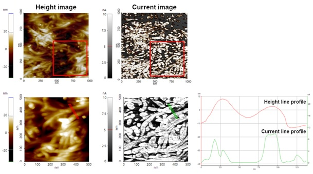
Figure 4. CNTs embedded polymer sample topography data (top left) and current distribution data (top right) acquired by C-AFM with a sample bias of U = + 0.3V. The inset red squares in each image were later re-scanned to demonstrate the resolution of this technique. CNTs embedded polymer sample topography data (bottom left) and current distribution data (bottom right) acquired from the lower-right red quadrant of the top’s scan area. The contrast levels of the current distribution data have been adjusted compared to the top images to increase the visibility of the CNT outlines. From the line profile of both height and current image, CNT can be distinguished with 15 nm ~ 20 nm in height and 7 nA ~ 9 nA in the current signal.
Conclusions
By detecting the current between a conductive AFM tip and the sample surface at a constant bias, conductive atomic force microscopy supplies researchers with access to both topography and electrical conductivity data simultaneously.
Regions of high conductivity enable a high current to pass from the sample to the tip. On the other hand, regions of low conductivity demonstrate a lower current flow between tip and sample. In addition to the sample topography, C-AFM detects the spatial variation of the current signal and images the current distribution.
In this study, a CNT embedded polymer sheet was characterized successfully using the Park NX10 system via C-AFM. At 1 µmx1 µm scan size and a sample bias of + 0.3 V, CNTs with a diameter of 14 nm and a relative current signal as high as 8 nA ~ 9 nA from the non-conductive surrounding polymer matrix could be clearly distinguished.
The data which was gathered in this study shows that this C-AFM can supply qualitative and quantitative information for the electrical characterization of advanced materials and devices.
References and Further Reading
- Rispal, L., Stefanov, Y., Wessely, F., and Schwalke, U., Carbon nanotube transistor fabrication assisted by topographical and conductive atomic force microscopy. Japanese journal of applied physics, 45 (4S) (2006) 3672.
- Conductive AFM (2016, Online Article). Retrieved from https://parksystems.com/park-spm-modes/94-electrical-properties/233-conductive-afm
- Saito, R., Dresselhaus, G., and Dresselhaus, M.S. (1998), Physical properties of carbon nanotubes, World Scientific.
- Phang, I. Y., Liu, T., Zhang, W. D., Schönherr, H., and Vancso, G. J., Probing buried carbon nanotubes within polymer–nanotube composite matrices by atomic force microscopy. European polymer journal, 43 (10) (2007) 4136-4142.
- PointProbe® Plus Contact Mode Short Cantilever -PtIr5 Coating (Online Article). Retrieved from https://www.nanosensors.com/pointprobe-plus-contact-mode-short-cantilever-ptir5-coating-afm-tip-PPP-CONTSCPt
Acknowledgments
Produced from materials originally authored by Vijaya Chalivendar, Professor in Mechanical Engineering, from University of Massachusetts at Dartmouth and Sze Yang, Professor in Chemistry, from University of Rhode Island.

This information has been sourced, reviewed and adapted from materials provided by Park Systems.
For more information on this source, please visit Park Systems.
