Close Menu
  • News
  • Medical
  • Technology
  • Nanomaterials
  • Research
  • Blog
    • Nasiol.com
  • Contact
    • Tech7685@gmail.com
What's Hot

Large-aperture MEMS modulator paves way for high-speed, energy-efficient optical communication systems

May 11, 2025

Dual-stage monitoring technique for nanocomposites can streamline manufacturing and property tracking

May 11, 2025

Probing the molecular mechanisms of metastasis

May 10, 2025
Facebook X (Twitter) Instagram
Nanotech – Nanomaterials | Medical | Research | News Stories Updated Daily Nanotech – Nanomaterials | Medical | Research | News Stories Updated Daily
  • News
  • Medical
  • Technology
  • Nanomaterials
  • Research
  • Blog
    • Nasiol.com
  • Contact
    • Tech7685@gmail.com
Facebook X (Twitter) Instagram
Nanotech – Nanomaterials | Medical | Research | News Stories Updated Daily Nanotech – Nanomaterials | Medical | Research | News Stories Updated Daily
Home»News»Combining graphene and nanodiamonds for better microplasma devices
News

Combining graphene and nanodiamonds for better microplasma devices

January 14, 2025No Comments4 Mins Read
Facebook Twitter Pinterest Telegram LinkedIn Tumblr WhatsApp Email
Combining graphene and nanodiamonds for better microplasma devices
Share
Facebook Twitter LinkedIn Pinterest Telegram Email
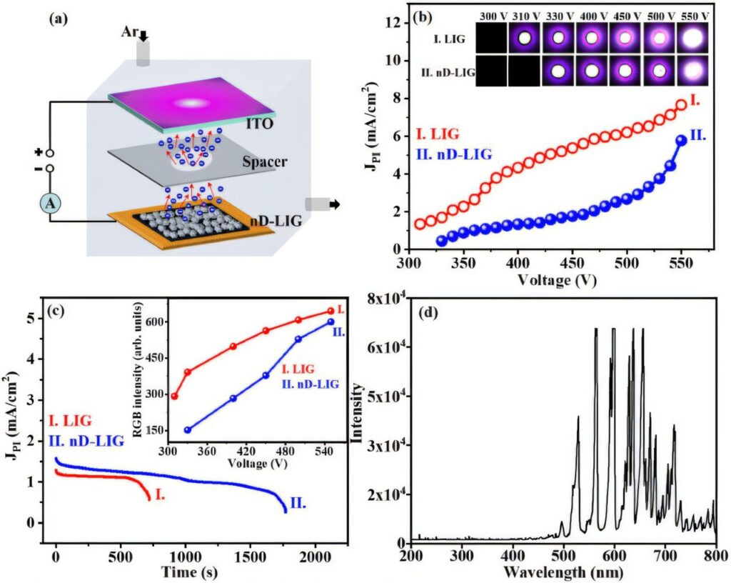
(a) Schematic of the microplasma device measurement. (b) plasma current density (JPI) versus applied voltage (V) of a microplasma cavity and the photographs of plasma illumination (PI) characteristics as inset, which utilized the ITO coated glass as anode and using either I. bare LIG or II. nD-LIG as cathode materials. (c) Lifetime plasma stability studies of I. LIG and II. nD-LIG. The inset of Fig. 4(c) shows the RGB intensity obtained from the PI photographs in the inset of Fig. 4(b). (d) Typical OES spectrum of Ar lines obtained from the micro discharges using nD-LIG as cathode in the microplasma device. Credit: Fundamental Plasma Physics (2024). DOI: 10.1016/j.fpp.2024.100047

Microplasma devices are incredibly versatile tools for generating and sustaining plasmas on micro- and millimeter scales. The latest advances in nanotechnology now promise to expand their range of applications even further but, so far, this progress has been held back by the limited stability of some nanostructures at the extreme temperatures required to sustain many plasmas.

In a recent study published in Fundamental Plasma Physics, K J Sankaran and colleagues at the CSIR Institute of Minerals and Materials Technology, Bhubaneswar, India, overcome this challenge by decorating sheets of graphene with more stable nanodiamonds—that is, diamonds with diameters smaller than about 100 nm—allowing them to endure far more extreme conditions.

This combined material could expand the use of microplasma devices across a diverse array of useful applications, such as sterilizing and healing wounds, analyzing chemicals, and displaying images.

Two forms of carbon

In a microplasma device, plasma is created by generating a strong electric field between a pair of electrodes—stripping electrons from the atoms and molecules in the space between them. In principle, graphene is the ideal material for these electrodes. Consisting of 2D sheets of carbon atoms, it has now been extensively studied since its initial characterization in the early 2000s.

“Graphene is renowned for its properties, including chemical stability and electrical conductivity,” Sankaran explains. “However, graphene has poor lifetime stability in severe plasma environments.”

One material which endures these conditions far more readily is diamond: a form of carbon with atoms arranged in a sturdy 3D lattice. “Diamond is known for its robust physical and chemical properties, and offers better stability for electron emission devices,” Sankaran says.

See also  Automated AFM Solutions for the Semiconductor Industry

If combined together, the properties of these two materials would be far better suited to use in microplasma electrodes—but as Sankaran explains, the integration process has proven difficult so far. “Previous attempts to integrate diamond and graphene have involved complex processes and high temperatures,” he says.

Seamless integration

In their study, Sankaran’s team presents an alternative approach to integrating these two forms of carbon as seamlessly as possible. Their method starts by irradiating a sheet of prerequisite material—usually polyimide or a similar carbon-rich polymer—with a powerful laser, causing its carbon atoms to rearrange themselves into graphene sheets. Graphene produced in this way is called laser-induced graphene (LIG).

“LIG presents itself as the quickest and simplest method for obtaining high-quality graphene utilizing commercially available and cost-effective instruments,” Sankaran explains. “Yet while LIG initially showed promising results for microplasma displays, it was observed to decay faster than anticipated.”

To prevent this decay, the researchers introduced a further step to the process. After preparing the LIG, they decorated its surface with diamonds, each just a few nanometers across.

They applied this step using a “drop-casting” technique: this involved seeding the growth of diamond nanocrystals inside a carbon-rich solution, placing a small droplet of the solution onto the LIG surface, and allowing it to dry. When applied this way, “the nanodiamond is not only uniform, but also enhances the quality of the graphene,” Sankaran says.

Boosting device performance

After assembling the material, the researchers could finally test its performance as the cathode in a practical microplasma device. The results were incredibly promising.

“The homogeneous fibrous structure of graphene embedded with nanodiamond showed significant stability in harsh plasma environments,” Sankaran says. “This enabled it to serve as a stable cathode for a long time.”

See also  Investigating and fine-tuning the properties of 'magic' graphene

Having demonstrated their easy and cost-effective technique, Sankaran’s team now hope it could soon be applied more widely for fabricating microplasma devices. This in turn could provide far easier access to their numerous benefits in research, medicine, and possibly even commercial applications in the not-too-distant future.


Source link

Combining Devices Graphene microplasma nanodiamonds
Share. Facebook Twitter Pinterest LinkedIn Tumblr Email

Related Posts

Large-aperture MEMS modulator paves way for high-speed, energy-efficient optical communication systems

May 11, 2025

Dual-stage monitoring technique for nanocomposites can streamline manufacturing and property tracking

May 11, 2025

Probing the molecular mechanisms of metastasis

May 10, 2025

AI-powered electronic nose detects diverse scents for health care and environmental applications

May 10, 2025

Microbubble dynamics in boiling water enable precision fluid manipulation

May 9, 2025

Unique molecule may lead to smaller, more efficient computers

May 9, 2025

Comments are closed.

Top Articles
News

Highly tunable biotemplating method expands nanostructure synthesis options

News

Radiation-Resistant Nanomaterials for Nuclear Systems

News

A smart solution for advanced wound care

Editors Picks

Large-aperture MEMS modulator paves way for high-speed, energy-efficient optical communication systems

May 11, 2025

Dual-stage monitoring technique for nanocomposites can streamline manufacturing and property tracking

May 11, 2025

Probing the molecular mechanisms of metastasis

May 10, 2025

AI-powered electronic nose detects diverse scents for health care and environmental applications

May 10, 2025
About Us
About Us

Your go-to source for the latest nanotechnology breakthroughs. Explore innovations, applications, and implications shaping the future at the molecular level. Stay informed, embrace the nano-revolution.

We're accepting new partnerships right now.

Facebook X (Twitter) Instagram Pinterest
Our Picks

Comprehensive model unravels quantum-mechanical effects behind photoluminescence in thin gold films

April 28, 2024

Researchers synthesize carbon nanotubes with precise chirality

November 2, 2024

How 2D materials could transform everyday electronics

November 27, 2024

Subscribe to Updates

Get the latest creative Nano Tech news from Elnano.com

© 2025 Elnano.com - All rights reserved.
  • Contact
  • Privacy Policy
  • Terms & Conditions

Type above and press Enter to search. Press Esc to cancel.

Cleantalk Pixel