Close Menu
  • News
  • Medical
  • Technology
  • Nanomaterials
  • Research
  • Blog
    • Nasiol.com
  • Contact
    • Tech7685@gmail.com
What's Hot

2D hybrid material integrates graphene and silica glass for next-generation electronics

June 4, 2025

Zeolite nanopore model links crystal size to metal cluster migration and catalyst performance

June 4, 2025

Spontaneous symmetry breaking in electron systems proves elusive

June 3, 2025
Facebook X (Twitter) Instagram
Nanotech – Nanomaterials | Medical | Research | News Stories Updated Daily Nanotech – Nanomaterials | Medical | Research | News Stories Updated Daily
  • News
  • Medical
  • Technology
  • Nanomaterials
  • Research
  • Blog
    • Nasiol.com
  • Contact
    • Tech7685@gmail.com
Facebook X (Twitter) Instagram
Nanotech – Nanomaterials | Medical | Research | News Stories Updated Daily Nanotech – Nanomaterials | Medical | Research | News Stories Updated Daily
Home»News»Automated technique for large-scale graphene transfer can boost electronic chip production
News

Automated technique for large-scale graphene transfer can boost electronic chip production

April 2, 2025No Comments3 Mins Read
Facebook Twitter Pinterest Telegram LinkedIn Tumblr WhatsApp Email
Automated technique for large-scale graphene transfer can boost electronic chip production
Share
Facebook Twitter LinkedIn Pinterest Telegram Email
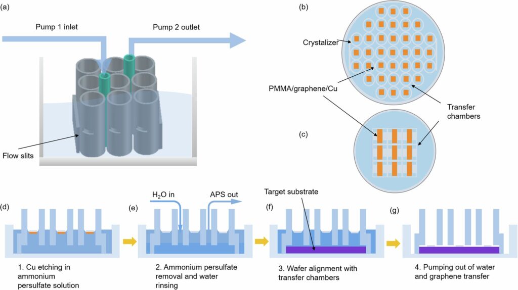
Apparatus for the automated, parallel transfer of an array of graphene ribbons. Credit: npj 2D Materials and Applications (2024). DOI: 10.1038/s41699-024-00491-8

The team led by Delphine Bouilly, a professor in UdeM’s Physics Department and director of IRIC’s Electronic Nanobiosensor Design and Application Research Unit, has developed an original technique for manipulating and moving graphene, a 1-atom-thick material involved in the assembly of electronic chips, for applications in molecular diagnostics. Led by doctoral student Amira Bencherif, the study was published in the journal npj 2D Materials and Applications.

Graphene is a two-dimensional (2D) nanomaterial composed of a single layer of carbon atoms. Its physical and electronic properties make it ideal for the manufacturing of a wide range of technological devices, such as biosensors.

It can be synthesized quickly and in large quantities on a copper surface, but the graphene ribbons must then be transferred from the metal surface to production disks (called wafers) to enable the simultaneous assembly of several chips. This transfer step is critical, and represents a major challenge for the large-scale production of devices based on 2D nanomaterials such as graphene.

To meet this need, Bouilly’s team has designed an original and novel graphene transfer technique. The transfer device consists of a network of glass chambers in which graphene-coated copper sheets are placed. By means of a pumping system, the chambers are filled, then emptied, with various solutions that dissociate the graphene from the copper and transfer it to a production wafer previously aligned with the chambers. The whole process is automated, with no manual handling, much like a miniature assembly line.

Manipulating the very small at large scale
Amira Bencherif and Delphine Bouilly Credit: IRIC

New manufacturing possibilities

The technique developed by Bouilly’s team offers several important advantages. It automates a manual method that used to require a great deal of dexterity, making it faster and easier to perform. The device also enables several graphene ribbons to be transferred in parallel, a key aspect in improving transfer speed and volume. In addition, the system enables vertical assembly of multiple graphene layers. Last but not least, automated parallel transfer saves on graphene usage by limiting losses.

See also  What is a Graphene Field Effect Transistor?

The system will facilitate the manufacturing of devices based on graphene and other 2D materials. At the same time, it will enable production volumes to be increased. The use of these devices as biosensors is currently being developed by the Bouilly laboratory, notably for the diagnosis of cancers and other diseases.

Provided by
University of Montreal


Source link

Automated boost Chip electronic Graphene largescale Production Technique transfer
Share. Facebook Twitter Pinterest LinkedIn Tumblr Email

Related Posts

2D hybrid material integrates graphene and silica glass for next-generation electronics

June 4, 2025

Zeolite nanopore model links crystal size to metal cluster migration and catalyst performance

June 4, 2025

Spontaneous symmetry breaking in electron systems proves elusive

June 3, 2025

Improving Crop Tolerance to Drought and Heat Using Nanomaterials

June 3, 2025

Crystal-modifying agent piracetam provides scalable strategy for high-efficiency all-perovskite tandem solar cells

June 3, 2025

Phonon decoupling in naturally occurring mineral enables subatomic ferroelectric memory

June 2, 2025

Comments are closed.

Top Articles
News

Magnesium protects tantalum, a promising material for making qubits

News

Special delivery nanoparticle can program stem cells while inside the body

News

Decoding the structure of nano ‘gene ferries’ to advance RNA drugs

Editors Picks

2D hybrid material integrates graphene and silica glass for next-generation electronics

June 4, 2025

Zeolite nanopore model links crystal size to metal cluster migration and catalyst performance

June 4, 2025

Spontaneous symmetry breaking in electron systems proves elusive

June 3, 2025

Improving Crop Tolerance to Drought and Heat Using Nanomaterials

June 3, 2025
About Us
About Us

Your go-to source for the latest nanotechnology breakthroughs. Explore innovations, applications, and implications shaping the future at the molecular level. Stay informed, embrace the nano-revolution.

We're accepting new partnerships right now.

Facebook X (Twitter) Instagram Pinterest
Our Picks

Exploring the Diversity of Semiconductor Building Blocks

January 8, 2024

Advancements in Amyloid-Beta Research for Neurodegenerative Conditions

July 23, 2024

Lipid Nanoparticle Formulation | A Guide

December 23, 2023

Subscribe to Updates

Get the latest creative Nano Tech news from Elnano.com

© 2025 Elnano.com - All rights reserved.
  • Contact
  • Privacy Policy
  • Terms & Conditions

Type above and press Enter to search. Press Esc to cancel.

Cleantalk Pixel