Close Menu
  • News
  • Medical
  • Technology
  • Nanomaterials
  • Research
  • Blog
    • Nasiol.com
  • Contact
    • Tech7685@gmail.com
What's Hot

2D hybrid material integrates graphene and silica glass for next-generation electronics

June 4, 2025

Zeolite nanopore model links crystal size to metal cluster migration and catalyst performance

June 4, 2025

Spontaneous symmetry breaking in electron systems proves elusive

June 3, 2025
Facebook X (Twitter) Instagram
Nanotech – Nanomaterials | Medical | Research | News Stories Updated Daily Nanotech – Nanomaterials | Medical | Research | News Stories Updated Daily
  • News
  • Medical
  • Technology
  • Nanomaterials
  • Research
  • Blog
    • Nasiol.com
  • Contact
    • Tech7685@gmail.com
Facebook X (Twitter) Instagram
Nanotech – Nanomaterials | Medical | Research | News Stories Updated Daily Nanotech – Nanomaterials | Medical | Research | News Stories Updated Daily
Home»News»A single atom can change the directional profile of the light emitted in scanning tunneling microscopes
News

A single atom can change the directional profile of the light emitted in scanning tunneling microscopes

November 13, 2024No Comments4 Mins Read
Facebook Twitter Pinterest Telegram LinkedIn Tumblr WhatsApp Email
A single atom can change the directional profile of the light emitted in scanning tunneling microscopes
Share
Facebook Twitter LinkedIn Pinterest Telegram Email
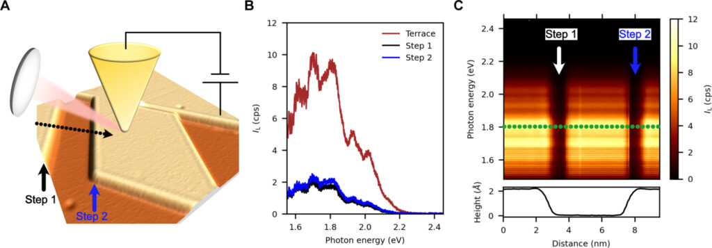
Raw light emission across a monoatomic height step in an STM nanocavity. Credit: Science Advances (2024). DOI: 10.1126/sciadv.adn2295

Researchers from Madrid explain a phenomenon that allows the direction of light emission to be controlled at the atomic scale. The paper provides a detailed explanation of how the profile of the light collected in a scanning tunneling microscope (STM) experiments changes when the tip is placed on an atomic step.

The properties of light in the far field are determined by what happens in the near field. The manipulation of light at the nanometer scale, below its wavelength, can be carried out in STM microscopes because the electromagnetic field is extremely confined between two metal nanostructures, the tip of the microscope and the sample, both separated by a typical distance of 1 nanometer. This configuration is called a nanocavity.

If an element is introduced into this nanocavity, such as an atomic defect, the system becomes a picocavity and has unique properties. It has been observed that, by introducing atomic steps into the nanocavities, it is possible to modify the direction of light emission in the experiments. This phenomenon, which researchers had previously observed, lacked a scientific explanation until now.

Researchers at IMDEA Nanociencia (Spain), led by Alberto Martín Jiménez and Roberto Otero, have made measurements of the radiated light in an experiment with a picoantenna composed of a gold STM tip and a smooth surface of silver atoms with an atomic step. The findings are published in the journal Science Advances.

During a typical measurement with an STM microscope, the tip travels across the sample, sweeping the surface back and forth as it picks up the signal. The researchers observed that the light emitted by each electron tunneling with the right energy on a monatomic step can be greater or less than that collected when the electron is injected into the atomically flat part of the surface.

See also  Fused molecules could serve as building blocks for safer lithium-ion batteries

By a comprehensive characterization of the light emitted by many steps, the researchers realized that the parameter that governs the intensity of light per electron is the relative orientation between the directions of the step and the direction of light collection, thus demonstrating that the emission of light is not equally distributed in all directions of space, but some are preferred to others with a cardioid-type directional profile.

In collaboration with researchers at IFIMAC-UAM, the authors elucidated the mechanism by which light emission is modified. In their work, they rationalize that in cavities as small as those between the tip and the STM sample an atomic size defect is enough to cause a significant redistribution of the electric field.

The effect is very different on both sides of the step, thus explaining why the angular profile of light emission depends on the orientation of the step. This phenomenon can be exploited to make a picoantenna, an element at the nanoscale with which to control the directionality of the emitted light.

Thus, in order to determine the electromagnetic field (light) emitted in the near field, it is not only necessary to take into account the point-sample structure of the microscope, but also the configuration and defects of the sample being swept, at the atomic scale, since a single atomic defect can modify the direction in which this radiation is emitted.

The authors see potential in this method to eventually tune the direction of light emission from molecules, quantum dots, or other quantum emitters. Investigating the optical properties of atomic objects is crucial not only to advance our knowledge but also to be able to design systems that have applications, for example, in quantum computing.

See also  Light-twisting materials created from nano semiconductors could be a game-changer for optics

Provided by
IMDEA Nanociencia


Source link

Atom Change directional emitted light microscopes profile Scanning Single Tunneling
Share. Facebook Twitter Pinterest LinkedIn Tumblr Email

Related Posts

2D hybrid material integrates graphene and silica glass for next-generation electronics

June 4, 2025

Zeolite nanopore model links crystal size to metal cluster migration and catalyst performance

June 4, 2025

Spontaneous symmetry breaking in electron systems proves elusive

June 3, 2025

Improving Crop Tolerance to Drought and Heat Using Nanomaterials

June 3, 2025

Crystal-modifying agent piracetam provides scalable strategy for high-efficiency all-perovskite tandem solar cells

June 3, 2025

Phonon decoupling in naturally occurring mineral enables subatomic ferroelectric memory

June 2, 2025

Comments are closed.

Top Articles
News

Quantum interference could lead to smaller, faster, and more energy-efficient transistors

Research

Breakthrough in Stretchable Graphene-Hydrogel Interfaces for Advanced Bioelectronics

Physicists track the mass and temperature of a levitated nanoparticle

Editors Picks

2D hybrid material integrates graphene and silica glass for next-generation electronics

June 4, 2025

Zeolite nanopore model links crystal size to metal cluster migration and catalyst performance

June 4, 2025

Spontaneous symmetry breaking in electron systems proves elusive

June 3, 2025

Improving Crop Tolerance to Drought and Heat Using Nanomaterials

June 3, 2025
About Us
About Us

Your go-to source for the latest nanotechnology breakthroughs. Explore innovations, applications, and implications shaping the future at the molecular level. Stay informed, embrace the nano-revolution.

We're accepting new partnerships right now.

Facebook X (Twitter) Instagram Pinterest
Our Picks

Graphene’s new ion permeability could transform water filtration and sensors

January 25, 2025

Synthesis of Covalent Organic Frameworks Thin Films

February 26, 2024

Polymeric nanomaterials can detect harmful substances in extreme environments

December 2, 2024

Subscribe to Updates

Get the latest creative Nano Tech news from Elnano.com

© 2025 Elnano.com - All rights reserved.
  • Contact
  • Privacy Policy
  • Terms & Conditions

Type above and press Enter to search. Press Esc to cancel.

Cleantalk Pixel