Close Menu
  • News
  • Medical
  • Technology
  • Nanomaterials
  • Research
  • Blog
    • Nasiol.com
  • Contact
    • Tech7685@gmail.com
What's Hot

Ballistic electrons chart a new course for next-gen terahertz devices

June 6, 2025

‘Stealthy’ lipid nanoparticles give mRNA vaccines a makeover

June 5, 2025

Single-layer waveguide display uses achromatic metagratings for more compact augmented reality eyewear

June 5, 2025
Facebook X (Twitter) Instagram
Nanotech – Nanomaterials | Medical | Research | News Stories Updated Daily Nanotech – Nanomaterials | Medical | Research | News Stories Updated Daily
  • News
  • Medical
  • Technology
  • Nanomaterials
  • Research
  • Blog
    • Nasiol.com
  • Contact
    • Tech7685@gmail.com
Facebook X (Twitter) Instagram
Nanotech – Nanomaterials | Medical | Research | News Stories Updated Daily Nanotech – Nanomaterials | Medical | Research | News Stories Updated Daily
Home»News»A novel avenue for engineering 2D MXene family via precious metals atomic layer deposition techniques
News

A novel avenue for engineering 2D MXene family via precious metals atomic layer deposition techniques

January 10, 2024No Comments3 Mins Read
Facebook Twitter Pinterest Telegram LinkedIn Tumblr WhatsApp Email
A novel avenue for engineering 2D MXene family via precious metals atomic layer deposition techniques
Share
Facebook Twitter LinkedIn Pinterest Telegram Email
Figure 1. A schematic of atomic layer deposition process and step coverage of ALD-Ru film. Credit: Advanced Science (2023). DOI: 10.1002/advs.202206355

A team of researchers, led by Professor Soo-Hyun Kim in the Graduate School of Semiconductors Materials and Devices Engineering and the Department of Materials Science and Engineering at UNIST has made significant progress in precisely controlling precious metals (Ru, Ir, Pt, Pd) incorporation by atomic layer deposition (ALD).

In this study, published in Advanced Science, the team successfully developed unique and unexplored two-dimensional (2D) nanomaterials V-MXene for the very first time coupled with precious metal ruthenium (Ru) through the ALD process. This breakthrough holds immense promise for various applications, both contact and non-contact mode of real-time temperature sensing at the human-machine interface.

The integration of Ru-engineered V-MXene through ALD has demonstrated a remarkable 300% enhancement in device sensing performance and durability, surpassing the capabilities of pristine V-MXene. This advancement not only paves the way towards the creation multifunctional, cutting-edge personal health care devices, but also holds great promises for the progression of clean energy conversion and storage technologies.

Moreover, the utilization of the industrially scalable ALD technique used in this research enables precise engineering of MXene surfaces with precious metals, thereby opening up new possibilities for future applications.

  • Engineering 2D MXene family via precious metals atomic layer deposition techniques
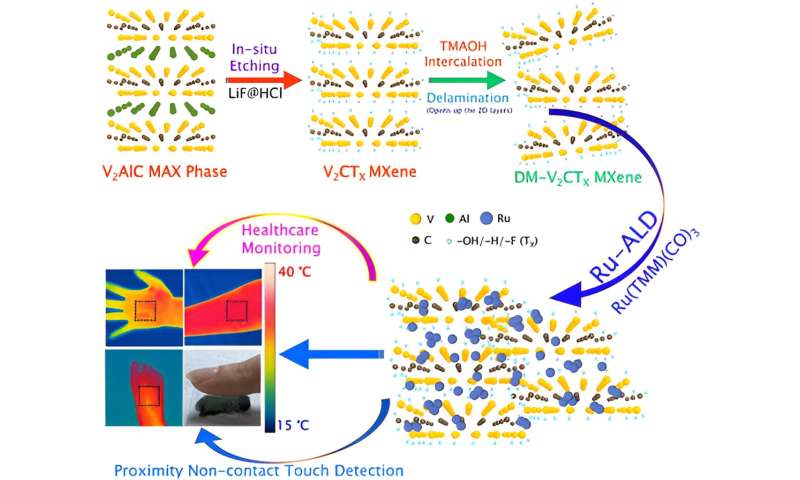
    Figure 2. As-synthesized bulk quantity delaminated V2CTX MXene (DM-V2CTX) to develop Ru-ALD Engineered DM-V2CTX (Ru@DM-V2CTX) for real-time skin temperature sensing, noncontact touch, proximity sensing, and breathing monitoring. Credit: Advanced Science (2023). DOI: 10.1002/advs.202206355
  • Engineering 2D MXene family via precious metals atomic layer deposition techniques
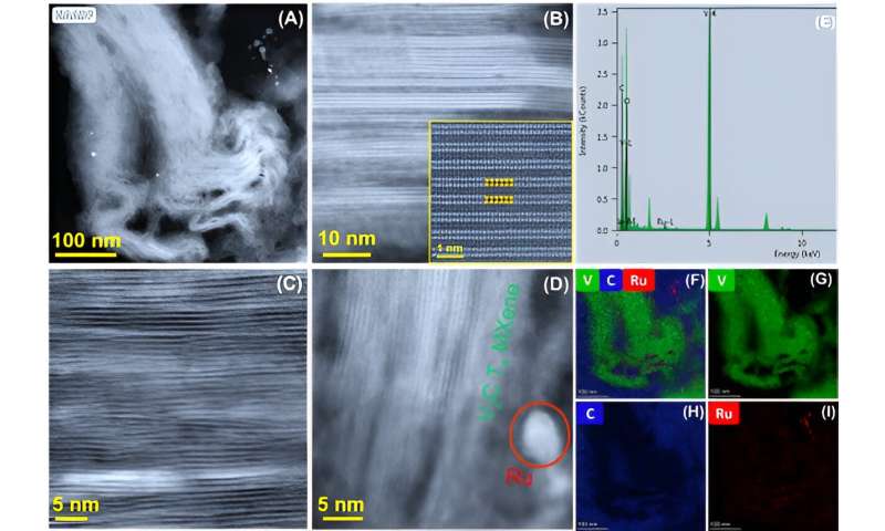
    Figure 3. Ru-ALD engineered DM-V2CTX MXene microstructure and elemental mapping. (A) HAADF STEM showing the presence of layered DM-V2CTX MXene structure and the distribution of Ru atoms/clusters, (B, C) HR-STEM of the well-defined layered structure of DM-V2CTX MXene throughout the sample and inset (B) confirms the opening of V2CTX MXene layers after the removal of Al-layers, (D) HR-STEM of both layered DM-V2CTX MXene and Ru lattices, (E) Super-X EDS elemental spectra confirming the elements V, C, Ru, and (F–I) their corresponding elemental mapping images. The atoms in Fig. 2B inset are shown with the same colors as illustrated in Figure 1 after the etching and delamination process. Credit: Advanced Science (2023). DOI: 10.1002/advs.202206355

“We are thrilled by the potential of this breakthrough,” said Professor Kim. “The precision-enabled integration of precious metals opens up a whole new world of possibilities in the development of versatile, next-generation, and safe personal health care devices, as well as clean energy conversion and storage systems, with the potential to substantially impact people’s lives.”

Dr. Debananda Mohapatra, an Associate Research Professor in the Graduate School of Semiconductors Materials and Devices Engineering at UNIST, emphasized the ease and versatility of engineering MXene surfaces with precious metals, using industrially favored ALD techniques. He also highlighted the potential for real-time applications in wearable health care devices and clean energy fields. He said, “This successful work marks the beginning of a thriving research field of focused on advancing 2D nanomaterials engineering and applications empowered by ALD.”

See also  New mass spectrometry technology could transform tiny sample analysis

The research team further highlighted the vast potential for exploring the less investigated non-Ti-MXenes, such as Mo, V, and Nb-based MXenes, for surface-internal structure engineering using selective precious metals (Ru, Ir, Pt, Pd) ALD processes.

By incorporating single atoms or atomic clusters of precious metals (Ru, Ir, Pt, and Pd), the resulting surface activity and the sensitivity/energy performance per atom can be significantly enhanced. This approach minimizes the use of these scarce and expensive precious metals.

Provided by
Ulsan National Institute of Science and Technology


Source link

atomic Avenue deposition engineering family layer metals MXene precious Techniques
Share. Facebook Twitter Pinterest LinkedIn Tumblr Email

Related Posts

Ballistic electrons chart a new course for next-gen terahertz devices

June 6, 2025

‘Stealthy’ lipid nanoparticles give mRNA vaccines a makeover

June 5, 2025

Single-layer waveguide display uses achromatic metagratings for more compact augmented reality eyewear

June 5, 2025

2D hybrid material integrates graphene and silica glass for next-generation electronics

June 4, 2025

Zeolite nanopore model links crystal size to metal cluster migration and catalyst performance

June 4, 2025

Spontaneous symmetry breaking in electron systems proves elusive

June 3, 2025

Comments are closed.

Top Articles
News

Semiconductor Manufacturing: The Industry’s Biggest Players

Medical

New AI-aided biosensor developed to detect neurodegenerative diseases

News

Nanoplastics put stress on trees and impair photosynthesis

Editors Picks

Ballistic electrons chart a new course for next-gen terahertz devices

June 6, 2025

‘Stealthy’ lipid nanoparticles give mRNA vaccines a makeover

June 5, 2025

Single-layer waveguide display uses achromatic metagratings for more compact augmented reality eyewear

June 5, 2025

2D hybrid material integrates graphene and silica glass for next-generation electronics

June 4, 2025
About Us
About Us

Your go-to source for the latest nanotechnology breakthroughs. Explore innovations, applications, and implications shaping the future at the molecular level. Stay informed, embrace the nano-revolution.

We're accepting new partnerships right now.

Facebook X (Twitter) Instagram Pinterest
Our Picks

New Quartet nanocage vaccine shows promise against coronavirus variants

May 9, 2024

From soot particle filters to renewable fuels: Examining carbon nanoparticle oxidation

January 31, 2025

Team makes breakthrough in high-energy particle detection

February 21, 2025

Subscribe to Updates

Get the latest creative Nano Tech news from Elnano.com

© 2025 Elnano.com - All rights reserved.
  • Contact
  • Privacy Policy
  • Terms & Conditions

Type above and press Enter to search. Press Esc to cancel.

Cleantalk Pixel