


Graphene is a single layer of atomic carbon arranged in a honeycomb lattice or hexagonal pattern. This nanomaterial is regarded as a ‘wonder’ material because of its high electron mobility, thermal conductivity, optical transparency, flexibility, strength, and a large specific surface area.1
Image Credit: marie_mi/Shutterstock.com
Graphene: Structure and Properties
A monolayered, planar structure of graphene with a honeycomb lattice is formed when carbon atoms share sp2 electrons with three neighboring carbon atoms. A bi-layered and tri-layered graphene structure is also present based on different stacking patterns. The flexibility and robustness of graphene nanoparticles are attributed to their overlapping sigma bonds with adjacent carbon atoms.2
The number of graphene layers determines specific properties. Both single-layer and bi-layer graphenes are zero band gap semiconductors because of the association between conduction and the valance bands at the Dirac points. However, it must be noted that the introduction of an electric field can open a band gap in bi-layered graphene. Few-layered graphene is composed of 2-10 carbon atom layers and exhibits a metallic structure with increasing layers.3
Graphene sheets are stacked in a crystallographic manner, which results in numerous stacking sequences. The stacking sequence of the honeycomb network determines the band structure and spin–orbit coupling of the graphene film.4
Graphene has many exceptional properties due to its structural features. Some of the key properties of graphene are discussed below.
Optical
The optical properties of graphene are based on its band structure, particularly interband electron transitions. The transmittance and reflectance properties of graphene at the optical region are dependent on the temperature, frequency, and carrier density. The transmittance property of graphene at the visible spectrum was found to be independent of frequency.5 A recent study has documented the superior non-linear optical response of graphene in an electromagnetic field.6
Electrical
The high electron mobility of graphene, i.e., 2 × 105 cm2/Vs, makes it a highly conductive material, even at room temperature. Graphene has a small overlap between the conduction and valance bands. The electronic dispersion around the Dirac point is linear and isotropic. The electronic homogeneity can be modulated by altering the graphene structure.7
Mechanical
Graphene exhibits exceptional stiffness, elasticity, strength, and toughness. The tensile strength of graphene is 125 GPa. A study has shown that graphene possesses around 100 times superior mechanical strength in comparison to steel.8
Understanding Electron Transport Properties of Graphene
To construct new graphene heterojunctions, it is imperative to understand its electron transport properties. The graphene sheets are composed of infinite numbers of aromatic rings that have zero energy gaps between valence and conduction bands. The intermediate molecules, such as perylene derivatives, are placed between these two extreme limits and they display many unique properties.9
The charged particles of graphene are chiral quasiparticles that have a linear Dirac-like dispersion, accounting for their electronic and transport properties. Due to the linear relationship between energy and momentum, the conduction and valence band intersect at the Dirac points at the Brillouin zone corners.
It must be noted that for neutral graphene, the chemical potential lies exactly at the Dirac points.10 The gate potential shifts the chemical potential away from the Dirac point and modifies the charge density of graphene. The linear dispersion of electrons and their tunability make graphene more dynamic than other two-dimensional semiconductor heterostructures.
In the ideal condition, i.e., graphene is without any impurities or structural defects, the mean free path of electrons is longer with negligible electrical resistivity. This condition results in ballistic conductivity or the highest electrical conductivity.11 However, an electron transport at the Dirac point results in minimal conductivity, even for ideal graphene. Essentially, electron transport in graphene qualitatively alters from metallic structures to suspended systems, where ballistic conduction occurs.
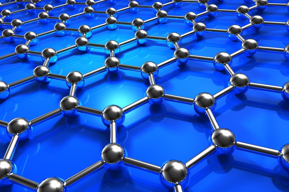
Image Credit: Oleksiy Mark/Shutterstock.com
Mechanisms of Electron Transport in Graphene
The electron transfer in graphene is broadly linked with the chemical reaction that leads to the relocation of electrons between graphene and other chemical structures. The chemical reagents either act as electron donors or acceptors.12 The electron transfer can involve chemical reagents or electrodes. In the case of electrodes-based electron transfer, graphene layers play varied roles in the electron transport reactions.
The free electrons in graphene participate during chemical reactions. This type of electron transfer is observed in aryl diazonium functionalization and selective oxidation of graphene.13 Other mechanisms that govern electron transfer involve the oxidation of graphene using molecular oxygen and ozone. Oxidation may also occur via plasma-based etching and liquid-phase oxidative etching.
The electron transport property of graphene is also effectively managed by the relativistic quantum theory. The presence of edges in graphene nanostructures, such as graphene nanoribbons, and graphene quantum dots, are associated with quantum confinement effects that result in unique electronic and optical properties.
Applications of Graphene in Electronics
Although graphene can be used to develop a new generation of miniaturized electronic devices, its application in the semiconductor industry is limited due to the absence of a band gap. Several strategies, such as doping and functionalization, have been employed to open the band gap, improving its applicability.
Graphene is used to develop various electronic sensors, which are applied for healthcare monitoring applications.14 A flexible piezoresistive-type pressure sensor has been fabricated using ultrathin wrinkled graphene film, and interdigital electrodes. This sensor exhibited higher sensitivity, reliability, and durability, than traditional graphene sensors. This type of pressure sensor could be used in robotics, medical diagnosis, and automatic electronics.
The optoelectronic properties and flexibility of graphene have been exploited for the development of portable and wearable electronics. These devices could be used to monitor human body signals and diseases. For instance, a non-invasive graphene electronic tattoo (GET)-based invisible electrooculography (EOG) sensor has been designed to assess the retina and cornea of human eyes.15
The electrophysiological properties of graphene are exploited for brain imaging. Due to the high transparency of graphene, these are used to fabricate a flexible and conductive wearable smart contact lens to monitor biomarkers of glucose contained in tears and intraocular pressure of individuals.
A Bottom-Up Approach To Graphene Synthesis
References and Further Reading
- Singh, S., et al. (2022) Graphene nanomaterials: The wondering material from synthesis to applications. Sensors International, 3, p. 100190. doi.org/10.1016/j.sintl.2022.100190
- Zhang, F., et al. (2022) Recent advances on graphene: Synthesis, properties and applications. Composites Part A: Applied Science and Manufacturing, 160, p. 107051. doi.org/10.1016/j.compositesa.2022.107051
- Moosa, A. A. & Abed, M. S. (2021) Graphene preparation and graphite exfoliation. Turkish Journal of Chemistry, 45(3), pp. 493-519. doi.org/10.3906/kim-2101-19 (Published 2021 Jun 30. )
- Yang, G., et al. (2018) Structure of graphene and its disorders: a review. Science and Technology of Advanced Materials, 19(1), pp. 613-648. doi.org/10.1080/14686996.2018.1494493. (Published 2018 Aug 29)
- Obraztsova, E., et al. (2021) Optical properties of graphene. Graphene (Second Edition), pp. 133-142. doi.org/10.1016/B978-0-08-102848-3.00006-2
- Yao, X., & Belyanin, A. (2012) Nonlinear optics of graphene in a strong magnetic field. ArXiv. doi.org/10.1088/0953-8984/25/5/054203
- Lee, J. H., et al. (2019) Electrical Property of Graphene and Its Application to Electrochemical Biosensing. Nanomaterials (Basel), 9(2), p. 297. doi.org/10.3390/nano9020297. (Published 2019 Feb 20)
- Papageorgiou, D. G., et al. (2017) Mechanical properties of graphene and graphene-based nanocomposites. Progress in Materials Science, 90, pp. 75-127. doi.org/10.1016/j.pmatsci.2017.07.004
- Guo, J., et al. (2023) Electron Transport Properties of Graphene/WS2 Van Der Waals Heterojunctions. Molecules, 28(19), p. 6866. doi.org/10.3390/molecules28196866
- Adam, S., et al. (2007) A self-consistent theory for graphene transport. Proceedings of the National Academy of Sciences of the United States of America, 104(47), pp. 18392-18397. doi.org/10.1073/pnas.0704772104
- Gosling, J. H., et al. (2021) Universal mobility characteristics of graphene originating from charge scattering by ionised impurities. Communications Physics, 4, p. 30. doi.org/10.1038/s42005-021-00518-2
- Rao, C., & Voggu, R. (2010) Charge-transfer with graphene and nanotubes. Materials Today, 13(9), pp. 34-40. doi.org/10.1016/S1369-7021(10)70163-2
- Ossonon, B. D., & Bélanger, D. (2017). Functionalization of graphene sheets by the diazonium chemistry during electrochemical exfoliation of graphite. Carbon, 111, pp. 83-93. doi.org/10.1016/j.carbon.2016.09.063
- Liu, J., et al. (2022) Applications of Graphene-Based Materials in Sensors: A Review. Micromachines (Basel), 13(2), p. 184. doi.org/10.3390/mi13020184. (Published 2022 Jan 26)
- Kireev, D., et al. (2022) Graphene electronic tattoos 2.0 with enhanced performance, breathability and robustness. Npj 2D Materials and Applications, 6(1), pp. 1-10. doi.org/10.1038/s41699-022-00324-6
