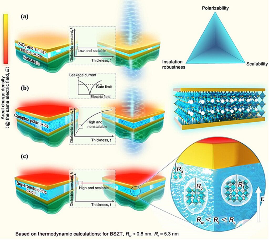
In our communication-centered society, Moore’s law sets a high expectation for the increasing rate of the packing density of Si-based transistors. This drives the search for thickness-scalable high dielectric constant (high k) gate layers. Current material candidates, from simple binary oxides to complex polar oxides, all have failed to solve the “polarizability-scalability-insulation robustness” trilemma, hence contributing to the sum total of issues threatening the continuation of the Moore’s law.
A team of material scientists led by Jun Ouyang from Qilu University of Technology in Jinan, China recently proposed a solution to this trilemma on gate layers, which is an ultrathin film of a ferroelectric oxide in its superparaelectric (SPE) state.
The team published their research article in Journal of Advanced Ceramics on April 30, 2024.
“In the SPE, its polar order becomes local and is dispersed in an amorphous matrix with a crystalline size down to a few nanometers, leading to an excellent dimensional scalability and a good field-stability of the k value,” said Jun Ouyang, senior author of the research article, professor in the School of Chemistry and Chemical Engineering and team leader of Advanced Energy Materials and Chemistry at Qilu University of Technology.
“As an example, a stable high k value (37±3) is shown in ultrathin SPE films of (Ba0.95,Sr0.05)(Zr0.2,Ti0.8)O3 (BSZT) sputter-deposited on LaNiO3-buffered Pt/Ti/ SiO2/(100)Si down to a 4 nm thickness at room temperature, leading to a small equivalent oxide thickness (EOT) of ~0.46 nm.”
The research team analyzed the average diameter of the nanometer polar clusters (NPCs), the feature size for the short-range ordered SPE film, as a function of the film thickness. They found that the film’s NPC size, which is positively correlated with the film’s k value, is dictated by the temperature of the sputter-deposition, not the film thickness.
“These observations suggest that the dominant factor for a scalable k in a SPE dielectric is its NPC size, not the film thickness usually being investigated. It is such a small feature size that has led to a good thickness scalability of k in a SPE ultrathin film, as opposed to a non-scalable k in its ferroelectric counterpart,” Jun Ouyang said.
“Furthermore, through studies of the temperature dependence of k (k–T curves), we estimated the critical NPC size for the superparaelectric-to-paraelectric (SPE-PE) transition in the BSZT film, i.e., its theoretical scalability limit as a gate layer. This limit is between 1.3 and 1.8 nm, which is consistent with the thermodynamic prediction for the BSZT material.”
The research team outlines other unique properties of the superparaelectric BSZT films endowed by their aforementioned microstructure of “well-dispersed nanometer polar clusters (NPCs)”.
These properties include a high breakdown strength (~10.5 MV·cm−1 for the 4 nm film), which ensures a low leakage current for the operation of the complementary metal oxide semiconductor (CMOS) gate. Moreover, a high electrical fatigue resistance, i.e., charge–discharge stability, was displayed by the SPE films. These results reveal a great potential of superparaelectric materials as gate dielectrics in the next-generation microelectronics.
The research team expects this work to spur development of new superparaelectric-based gate layers to further decrease the EOT value and help continue Moore’s law.
Provided by
Tsinghua University Press


