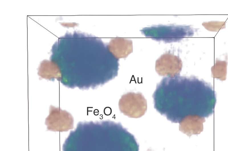
By exploiting a smart learning algorithm that fuses two microscopy signals, University of Michigan researchers have accomplished high-resolution, efficient 3D chemical imaging for the first time at the one-nanometer scale. For context, a nanometer is one-millionth of a millimeter, or one-hundred-thousandth the width of a human hair.
“Seeing invisible worlds, far smaller than the wavelengths of light, is absolutely critical to understanding the matter we are engineering at the nanoscale, not just in 2D but in 3D as well,” said Robert Hovden, an associate professor of materials science and engineering at U-M and corresponding author on the study published in Nature Communications.
“By leveraging our knowledge of the imaging process and taking a new approach to tomographic reconstruction, we are now able to simultaneously image structure and chemical composition with high resolution in 3D. This is an especially useful approach for complex and heterogeneous materials,” said Mary Scott, contributing author on the study and the Ted van Duzer Associate Professor of the UC Berkeley Department of Materials Science and Engineering and faculty staff scientist in the Molecular Foundry Division of the Lawrence Berkeley National Laboratory.
Up to this point, nanomaterial researchers have had to choose between imaging 3D structure or 2D chemical distribution.
Both imaging techniques use a scanning transmission electron microscope, which accelerates a high energy electron beam through a sample material. These high energy electrons can resolve structures at distances smaller than the bond-length of atoms. However high-resolution imaging requires a substantial amount of dose, or energy, to efficiently capture atomic structure or chemistry.
Most often, the dose required for chemical imaging is right at the material’s limitation where samples will begin to melt if exposed to the beam any longer. This is especially consequential for 3D chemical imaging, which requires the acquisition of many chemical images.
Nanoscale 3D imaging works similarly to a medical CT scan, where equipment swivels around a patient to collect images at multiple angles to view internal structures in 3D.
Instead with electron tomography—the favored method for 3D nanoscale imaging—the electron beam remains stationary while the sample tilts around it. However this comes with its own set of complications, where researchers are unable to fully image their sample and must rely on machine learning algorithms to predict views at unavailable angles.
“Structure is one thing, but if you wanted to see the oxide layer on a transistor or the distribution of oxygen in a nanoparticle engineered for clean energy applications, you need to see chemistry at the nanoscale, which you can’t get from electron tomography alone,” said Hovden.
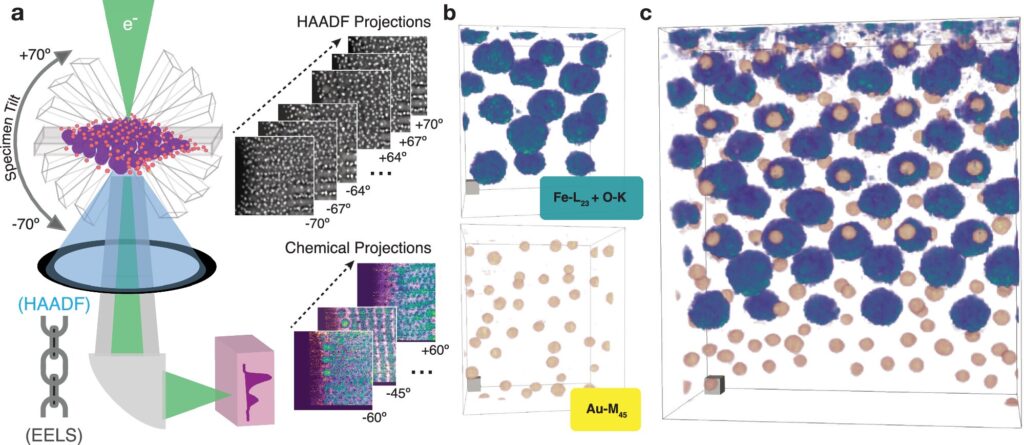
To overcome the energy dose issue, the research team developed a new process known as “multi-modal electron tomography” to collect images at every tilt angle while chemical images are sparsely collected every few tilts. A multi-modal algorithm then takes the information for both signal types and outputs the 3D structure and chemistry.

Mixing signals allows about a 100 times energy dose reduction, ensuring the sample is not destroyed before imaging is complete.
Results demonstrate the technique is capable of imaging both organic compounds and metals simultaneously, proving the technique’s use on a broad range of materials.
“Our solution takes advantage of all the complementary signals that are present in our microscope by promoting communication between a signal that doesn’t require much dose and a very dose hungry signal,” said Jonathan Schwartz, a doctoral graduate of materials science and engineering from U-M and lead author of the study.
The two imaging techniques rely on different physical properties of electrons as they move through a material. 3D imaging relies on elastic scattering, where electrons do not lose energy as they pass through the sample. In chemical imaging, the higher energy electron beam increases the likelihood of the rarer event of inelastic scattering, where electrons lose a specific amount of energy that reflects the element it collided with, providing a unique chemical signature.
“This is a radically new approach to how we mix and use signals of elastically and inelastically scattered electrons,” said Hovden.
In addition to the chemical distribution, the machine learning output even provides information about stoichiometry, or the ratios of elements in the material. For example, for every motif in ferric oxide (Fe2O3), you could have two iron atoms for every three oxygen atoms, or you could maybe have two iron atoms for every two oxygen atoms.
“Because the algorithm is trying to figure out the decomposition of the elements present, it captures the ratio of chemistries quite well. That was something we got for free as part of our algorithm’s optimization process,” said Schwartz, now a scientist at the Chan Zuckerberg Imaging Institute.
Hovden credits the technique’s success to leveraging physics, materials science and modern computer science.
“The first step is to understand the physics of the electrons interacting with the matter under our microscope for each detector. Computer science links all of these detectors together to create a complete image. It’s a brand new space to play in this field,” said Hovden.
Combining two different signals to enhance information—also known as multimodal imaging—is gaining traction across engineering fields. Methane leaks can be detected and addressed using satellite imaging combined with thermal or chemical sensing. Self driving cars mix remote sensing signals, which provide terrain information, with signals from the car to improve navigation.
“This is one of the first big results of the power of multimodality in our field. It’s exciting to still find new ways to see matter at these small scales,” said Hovden.


