Close Menu
  • News
  • Medical
  • Technology
  • Nanomaterials
  • Research
  • Blog
    • Nasiol.com
  • Contact
    • Tech7685@gmail.com
What's Hot

Flux Tools for Drift Conditions

May 20, 2025

Bringing superconducting nanostructures to 3D

May 20, 2025

Next Generation Magnetic Force Microscopy

May 19, 2025
Facebook X (Twitter) Instagram
Nanotech – Nanomaterials | Medical | Research | News Stories Updated Daily Nanotech – Nanomaterials | Medical | Research | News Stories Updated Daily
  • News
  • Medical
  • Technology
  • Nanomaterials
  • Research
  • Blog
    • Nasiol.com
  • Contact
    • Tech7685@gmail.com
Facebook X (Twitter) Instagram
Nanotech – Nanomaterials | Medical | Research | News Stories Updated Daily Nanotech – Nanomaterials | Medical | Research | News Stories Updated Daily
Home»News»Bringing superconducting nanostructures to 3D
News

Bringing superconducting nanostructures to 3D

May 20, 2025No Comments3 Mins Read
Facebook Twitter Pinterest Telegram LinkedIn Tumblr WhatsApp Email
Bringing superconducting nanostructures to 3D
Share
Facebook Twitter LinkedIn Pinterest Telegram Email
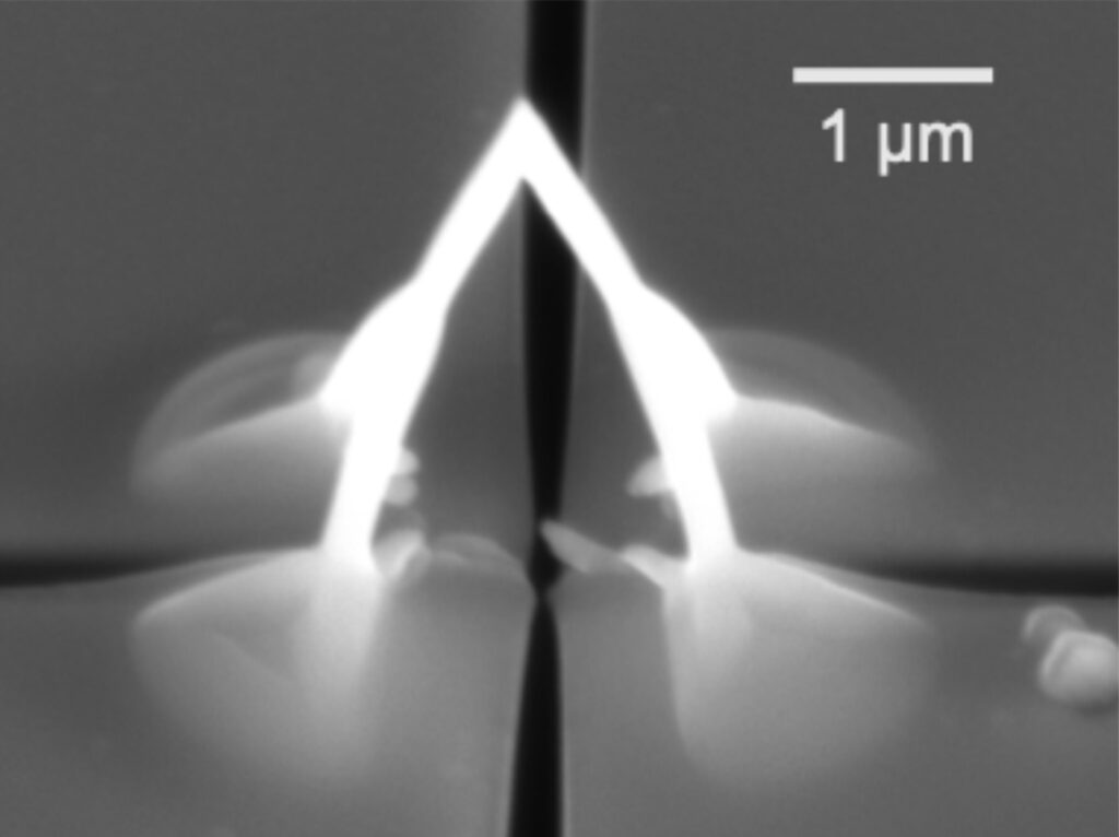
Scanning electron microscope image of a three dimensional superconducting nanostructure (nanobridge) deposited using direct-write 3D nanoprinting. Credit: MPI CPfS

The move from two to three dimensions can have a significant impact on how a system behaves, whether it is folding a sheet of paper into a paper airplane or twisting a wire into a helical spring. At the nanoscale, 1,000 times smaller than a human hair, one approaches the fundamental length scales of, for example, quantum materials.

At these length scales, the patterning of nanogeometries can lead to changes in the material properties itself—and when one moves to three dimensions, there come new ways to tailor functionalities, by breaking symmetries, introducing curvature, and creating interconnected channels.

Despite these exciting prospects, one of the main challenges remains: how to realize such complex 3D geometries, at the nanoscale, in quantum materials? In a new study, an international team led by researchers at the Max Planck Institute for Chemical Physics of Solids have created three-dimensional superconducting nanostructures using a technique similar to a nano-3D printer.

They achieved local control of the superconducting state in a 3D bridge-like superconductor, and could even demonstrate the motion of superconducting vortices—nanoscale defects in the superconducting state—in three dimensions. The work has been published in the journal Advanced Functional Materials.

Superconductors are materials that are renowned for their ability to exhibit zero electrical resistance and expel magnetic fields. This striking behavior arises from the formation of so-called Cooper pairs—bound pairs of electrons that move coherently through the material without scattering.

“One of the main challenges involves gaining control over this superconducting state at the nanoscale, which is key for the exploration of novel effects, and the future development of technological devices” explains Elina Zhakina, postdoctoral researcher at the MPI-CPfS, and first author of the study.

See also  Advances in nanoscale force measurement opens doors to unprecedented biological insights

When patterning superconductors in 3D nanogeometries, the international team, involving researchers from Germany (MPI CPfS, IFW) and Austria (TU Wien, University of Vienna), were able to locally control the superconducting state—i.e., “switching off” the superconductivity in different parts of the nanostructure.

This coexistence of superconducting and “normal” states can lead to quantum mechanical effects, such as so-called weak links, used for example for ultra-sensitive sensing. However, until now, such control has typically required the design of structures, for example, in planar thin films, where the coexistence of states is predetermined.

“We found that it is possible to switch on and off the superconducting state in different parts of the three-dimensional nanostructure, simply by rotating the structure in a magnetic field,” said Claire Donnelly, Lise Meitner Group leader at the MPI-CPfS and last author of the work. “In this way, we were able to realize a ‘reconfigurable’ superconducting device.”

This realization of reconfigurable functionality offers a new platform for building adaptive or multi-purpose superconducting components. This, along with the ability to propagate defects of the superconducting state, opens the door to complex superconducting logic and neuromorphic architectures, setting the stage for a new generation of reconfigurable superconducting technologies.

Provided by
Max Planck Society


Source link

Bringing Nanostructures superconducting
Share. Facebook Twitter Pinterest LinkedIn Tumblr Email

Related Posts

Flux Tools for Drift Conditions

May 20, 2025

Next Generation Magnetic Force Microscopy

May 19, 2025

Sulfur-capped carbon nanobelts promise novel applications

May 19, 2025

Self-assembled dodecahedral nanostructure features 60 metal ions and peptide ligands

May 19, 2025

In vivo 3D printing using sound holds promise for precise drug delivery, wound healing and more

May 18, 2025

Sub-millimeter waveguide shrinks augmented-reality glasses

May 17, 2025

Comments are closed.

Top Articles

Novel bioluminescent immunosensor shows promise for quantitative point-of-care testing

News

Gold nanoparticles found to reverse brain deficits in multiple sclerosis and Parkinson’s

News

A new fullertube molecule is found

Editors Picks

Flux Tools for Drift Conditions

May 20, 2025

Bringing superconducting nanostructures to 3D

May 20, 2025

Next Generation Magnetic Force Microscopy

May 19, 2025

Sulfur-capped carbon nanobelts promise novel applications

May 19, 2025
About Us
About Us

Your go-to source for the latest nanotechnology breakthroughs. Explore innovations, applications, and implications shaping the future at the molecular level. Stay informed, embrace the nano-revolution.

We're accepting new partnerships right now.

Facebook X (Twitter) Instagram Pinterest
Our Picks

Boron nitride-based nanocomposites have unexpected properties, researchers discover

August 14, 2023

Redefining Nanoscale Analysis with FusionScope

October 6, 2023

Engineering perovskite materials at the atomic level paves way for new lasers, LEDs

October 21, 2024

Subscribe to Updates

Get the latest creative Nano Tech news from Elnano.com

© 2025 Elnano.com - All rights reserved.
  • Contact
  • Privacy Policy
  • Terms & Conditions

Type above and press Enter to search. Press Esc to cancel.

Cleantalk Pixel