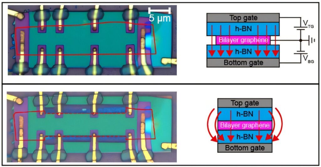
Electron transport in bilayer graphene exhibits a pronounced dependence on edge states and a nonlocal transport mechanism, according to a study led by Professor Gil-Ho Lee and Ph.D. candidate Hyeon-Woo Jeong of POSTECH’s Department of Physics, in collaboration with Dr. Kenji Watanabe and Dr. Takashi Taniguchi at Japan’s National Institute for Materials Science (NIMS).
The findings are published in the journal Nano Letters.
Bilayer graphene, comprising two vertically stacked graphene layers, can exploit externally applied electric fields to modulate its electronic band gap—a property essential for electron transport. This distinctive feature has drawn considerable attention for its prospective role in “valleytronics,” an emerging paradigm for next-generation data processing.
By capitalizing on the “valley,” a quantum state in an electron’s energy structure that functions as a discrete data storage unit, valleytronics enables faster, more efficient data handling than conventional electronics or spintronics. With its tunable band gap, bilayer graphene stands as a foundational platform for advanced valleytronics research and device innovation.
A central concept in valleytronics is the “Valley Hall Effect (VHE),” which describes how electron flow is selectively channeled through discrete energy states—known as “valleys”—within a given material. Consequently, a remarkable phenomenon called “nonlocal resistance” emerges, introducing measurable resistance in regions lacking direct current flow—even in the absence of conduction paths.
While much of the current literature regards nonlocal resistance as definitive proof of the VHE, some researchers posit that device-edge impurities or external factors—such as manufacturing processes—may also produce the observed signals, leaving the debate over VHE’s origins unresolved.
To ascertain the definitive source of nonlocal resistance in bilayer graphene, the joint POSCO-NIMS research team fabricated a dual-gate graphene device, enabling precise band gap control. They subsequently compared the electrical characteristics of pristine, naturally formed graphene edges with those artificially processed using Reactive Ion Etching.
The finding revealed that nonlocal resistance in naturally formed edges conformed to theoretical expectations, while etching-processed edges exhibited nonlocal resistance exceeding those values by two orders of magnitude.
This discrepancy indicates that the etching procedure introduced extraneous conductive pathways unrelated to the VHE, thereby explaining why a reduced band gap had been observed in prior measurements of bilayer graphene.
“The etching process, a vital step in device fabrication, has not received sufficient scrutiny, particularly regarding its impact on nonlocal transport,” commented Hyeon-Woo Jeong, the paper’s first author.
“Our findings underscore the need to reexamine these considerations and offer crucial insights for advancing valleytronics device design and development.”


