A research team has successfully developed a new technology to control doping at the nucleus (seed) phase to increase the performance of semiconductor nanocrystals. The study uncovered how the doping process and location differ depending on the type of doping element (dopant). The developed technology is expected to be widely utilized in advanced electronic devices, such as displays and transistors.
With the rapid development of advanced technologies in recent years, such as displays and transistors, interest in technologies that can precisely control doping in nanoscale semiconductors is growing. In particular, II-VI semiconductor-based nanocrystals have been widely studied owing to their outstanding optical and electrical properties.
While doping plays a critical role in semiconductor technology, the problem of low doping efficiency in small semiconductors, such as nanocrystals, remains. This problem arises because dopants tend to be absorbed onto the surface of a semiconductor during its growth and do not penetrate its interior effectively.
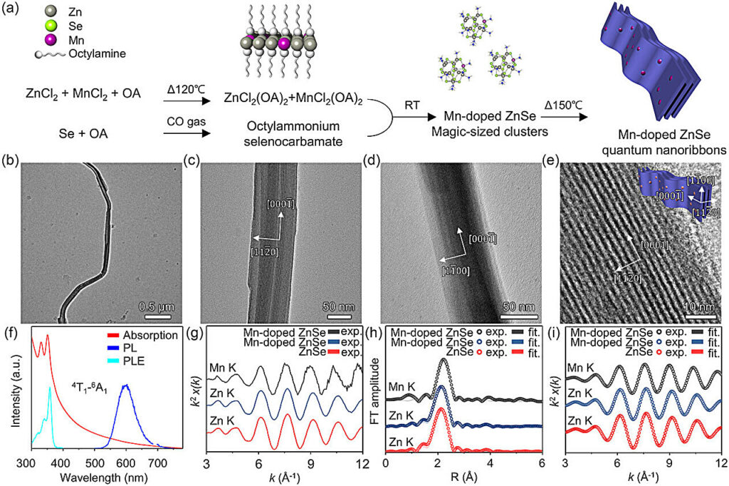
In this context, DGIST Professor Jiwoong Yang’s research team developed a controlled nucleation doping method, which induces doping at the “nanocluster” phase, a stage preceding nanocrystal growth. Using this technique, the team successfully implemented stable and precise doping in ZnSe semiconductor nanocrystals and identified the reasons behind the variations in doping processes and locations depending on the dopant type.
The work is published in the journal Small Science.
Although previous studies on doping II-VI semiconductor nanocrystals have mainly used CdSe, a heavy metal, Cd is harmful to the environment and has poor stability. This study developed a technology applicable to nanocrystals that eliminates the use of heavy metals, demonstrating its potential for practical applications while also addressing environmental concerns. In addition, the study demonstrated the technology’s applicability across various electronic devices, such as displays and transistors.
Professor Yang said, “This research has enabled us to systematically establish doping control technology in nanocrystals. The findings will not only serve as important foundational data for designing and fabricating optoelectronic devices, such as next-generation displays and transistors, but also open up new possibilities for designing innovative devices through precise doping control technology.”
This study was conducted in collaboration with a research team led by Stefan Ringe at the Department of Chemistry, Korea University (Dongwon Kim).


