Graphene has lived up to its promise in the lab. Now, EU researchers are working on supporting its wider adoption in high-end electronics, photonics and sensors.
Dr. Inge Asselberghs has been closely involved in advanced graphene research over the past decade. Today, she’s at the forefront of efforts to bring this “miracle material” out of the lab and into society.
Asselberghs is part of an international team of researchers that set up a prototype manufacturing facility for graphene and other 2D materials at Imec, a leading global nanoelectronics research institute based in Leuven, Belgium.
The team pools expertise from 11 universities, research institutes and companies in six European countries as part of the 2D experimental pilot line (2D-EPL). Their aim is to advance the production and integration of graphene in prototypes for use in high-end electronics, photonics and sensors.
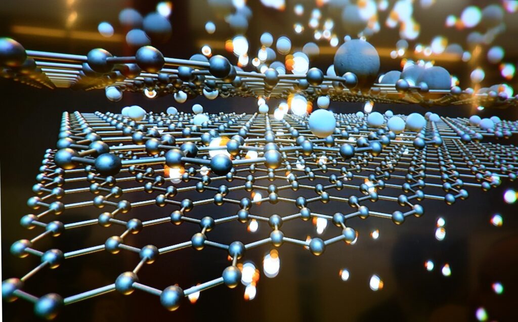
Graphene has the potential to fundamentally transform many areas of technology. Consisting of just a single layer of carbon atoms, it is extremely thin.
Graphene is exceptionally strong, light and flexible, and able to conduct both heat and electricity. This makes it highly adaptable for a wide range of products, from next-generation batteries to advanced aeronautic and space applications.
“The hype started as soon as graphene was discovered. It was much stronger than initially anticipated,” said Asselberghs.
Recognizing the economic potential of graphene and other 2D materials, the EU launched the 10-year Graphene Flagship initiative in 2013, bringing together 178 academic and industrial partners with a budget of €1 billion to boost research in this area. 2D-EPL is part of this wide-ranging initiative.
Experimental prototypes
The aim of the experimental pilot line, set up in multiple locations, was to accelerate the use of graphene and other layered materials in the manufacture of new prototypes for electronics, photonics, sensors and optoelectronics. This will be a crucial step before 2D materials can be integrated into full-scale chip manufacturing.
“Our first goal was to figure out how to make graphene devices on a wafer scale by modifying existing processes so that they can be handled in automated fabrication facilities,” said Asselberghs.
Wafers are thin round slices of material for use in electronics and other industries. Reaching the stage where graphene can be routinely included in sophisticated devices would be a major milestone.
Flawless manufacturing
One drawback is that the thinness of graphene and other 2D materials can make them tricky to manufacture flawlessly. It takes only a speck of dust, or even a few unwanted molecules, to cause defects in graphene.
During the manufacturing process, graphene must be protected by a thin polymer layer and then transferred to a silicon base. These thin layers need to be handled extremely carefully. Figuring out how to do this in an automated process was a challenge.
“Your room and your tools need to be super-controlled and clean to avoid any particles on your device,” Asselberghs said.
An assembly line was set up in Imec’s special fabrication facility to process wafers with graphene that are 200 or 300 mm across, a standard size used in silicon fabrication facilities and therefore familiar to industry.
Other research partners added tools, machines and knowledge to help “cook up” the perfect graphene recipe, as large-scale manufacture remains delicate.
Discover the latest in science, tech, and space with over 100,000 subscribers who rely on Phys.org for daily insights.
Sign up for our free newsletter and get updates on breakthroughs,
innovations, and research that matter—daily or weekly.
Exciting potential
Europe has been a global leader in exploring the potential of graphene and other 2D materials.
“We are in a pretty strong position in Europe with 2D materials because we’ve had consistent long-standing funding for this research,” said Harm Knoops, a Dutch researcher with Oxford Instruments Plasma Technology from Bristol, UK.
His company specializes in the use of plasma technology for the creation and manipulation of matter with atomic-scale accuracy and contributed to the manufacturing process in 2D-EPL.
The excitement among researchers and industries around 2D materials is not focused only on graphene. The researchers are also interested in other super thin materials that can—like silicon—act as semiconductors and be used in advanced manufacturing.
The potential of these materials has attracted interest from many areas of industry. Potential customers have already been in touch with the research team with specific design requests.
On the cusp
A big advantage of graphene is that it consists of carbon, one of the most common elements on Earth. The hope is that the integration of graphene will support the cheap and large-scale manufacture of advanced electronics and sensors, and allow the development of devices that haven’t even been invented yet.
Although it is not yet ready for industrial roll-out as part of advanced electronics, graphene and other 2D materials are certain to reach the market eventually. They could lead to better devices with super-fast transistors or sharper sensors, said Knoops, whose company was part of the Graphene Flagship.
“It could mean data centers use less power, or your internet is faster, or you can have a special sensor or medical device connected to your phone.”


