Researchers have developed a breakthrough technology that uses light to visualize nanoscale glass microcapillary tips, enabling precise and delicate contact with other objects.
A “microcapillary” is a precision tool with a very small aperture (0.1 mm to 0.000010 mm in diameter) fabricated from a glass tube. It is utilized as a vital tool in various fields, from biotechnology to manipulating cells, to micro-electroplating and nano-3D printing.
Specifically, it is used in biotechnology for tasks such as injecting sperm into an egg during in vitro fertilization (IVF) or as a tool for penetrating cell membranes to study cellular mechanisms. In electroplating, it allows metal plating within extremely small areas, which is useful for manufacturing precision electronic circuits or microstructures. It can also be used as a 3D printing nozzle to print ultra-fine structures in three dimensions.
A primary concern in utilizing microcapillaries is to ensure delicate and precise contact at the sharp tip so that the glass microcapillary does not break or the target object is not damaged. In the past, contact was determined by observing with an optical microscope, but for nanoscale ultra-fine microcapillaries, contact could not be determined due to the diffraction-limited resolution.
Although other methods, such as monitoring electrical current or mechanical vibrations have been employed, their versatility is constrained by material specificity (limited to conductive materials) or by interference that can potentially influence the results.
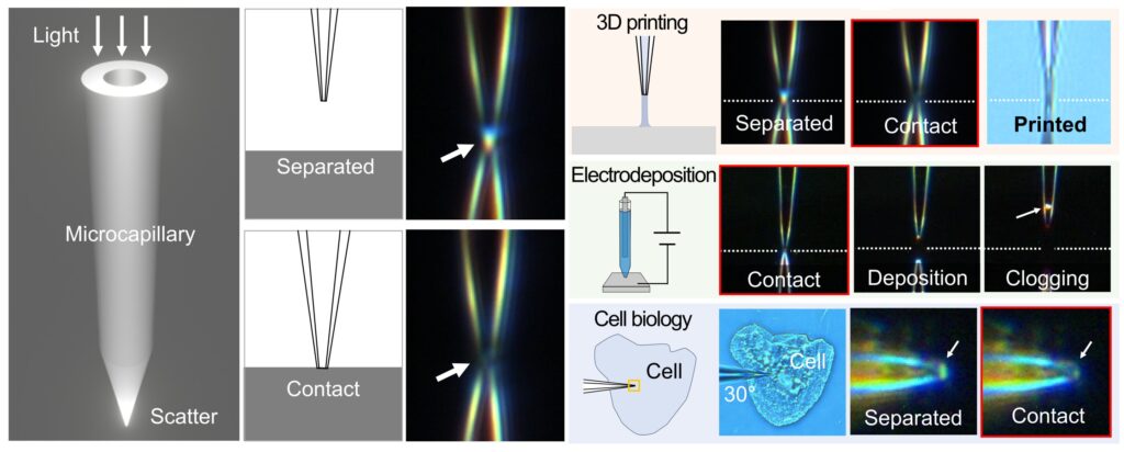
The new method developed by Dr. Jaeyeon Pyo’s team utilizes light. When light is projected into a glass microcapillary tube, the light travels through the tube to the sharp end tip. When the tip does not touch an object, a bright scattering light is observed, and the moment it touches an object, it immediately disappears. This simple method, which only requires one light source to surpass the resolution limits of optical microscopes for contact detection, is a remarkable achievement that cannot be accomplished without a comprehensive understanding of the light-matter interactions at the nanoscale.

The research team discovered through various experiments and simulations that light, which had been transmitted in the form of an evanescent wave, is not scattered at the tip upon contact, but rather transmitted to the object it contacts. To validate the applicability of this technology, they showcased the precise contact detection capabilities of the micro-glass tube in various fields, including nano-3D printing processes, micro copper electroplating processes and clogging solutions, and the invasion of cell walls in oral epithelial cells, confirming its accurate and immediate detection performance.
Through various experiments and simulations, the research team discovered that the light, which is propagating in the form of an evanescent wave, is transferred to the object that has come into contact rather than being scattered at the tip.
To validate the applicability of this technology, the team demonstrated the delicate contact of microcapillaries in various fields, such as the nanoscale 3D printing process, the micro electroplating process of copper, solving the clogging of nozzles, and the invasion of membranes of oral epithelial cells, confirming its precise and immediate detection performance.
The research was published as a cover article in ACS Nano.
Dr. Jaeyeon Pyo explained the background of the research, stating, “As the previously developed nanoscale 3D printing process, based on optical microscopic observation, faced physical limitations, a completely new approach was needed to improve the resolution, stability, and yield.
“With an understanding of optical physics at the nanoscale, we came up with a groundbreaking idea to utilize the 3D printing nozzle as a tool for monitoring its contact, which led to successful results.”
Having completed the patent application for the original technology, KERI expects this breakthrough to attract significant interest from various research institutes and industries that require nanoscale precision processes, such as 3D printing, displays, biotechnology, electroplating, and microelectronics.
The simplicity of the technology, which can be implemented by using just a single light source without material or environmental limitations, suggests a wide range of potential applications. Dr. Jaeyeon Pyo’s team plans to further demonstrate and validate its applicability in more fields, actively discover companies in demand, and pursue technology transfer.


